Time:2026-05-20Reading:1102Second
As AI big models, autonomous driving, and computing power clusters become high-frequency buzzwords in the technology industry, the golden track of AI chips is expanding at an astonishing speed. However, every high-performance AI chip, from its design blueprint to practical application, cannot do without a key "quality inspection pass" - the semiconductor high-frequency needleAccurate verification. These seemingly tiny precision devices, like the "microscopic stethoscope" of the chip industry, safeguard the performance and reliability of chips with high precision, becoming an indispensable core support behind the rise of the AI chip race.
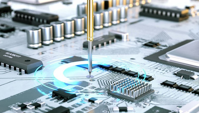
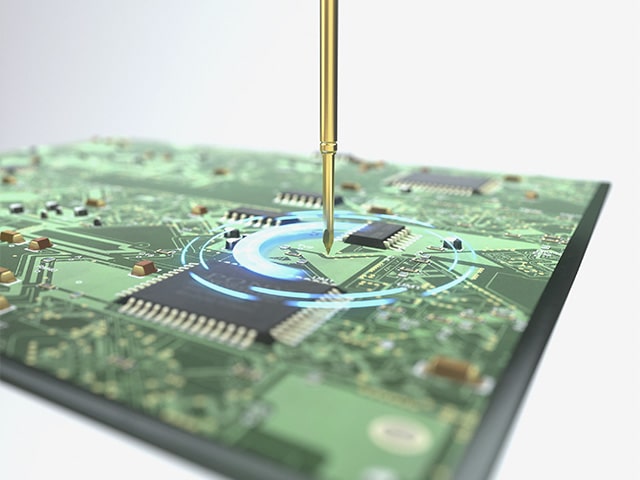
In the semiconductor industry chain, although probes are compact, they are essential core consumables in the testing process. It connects one end to a chip pin (or wafer solder ball) and the other end to a testing machine, accurately transmitting electrical signals to detect the conductivity, current stability, functional integrity, and even aging performance of the chip in high temperature environments.

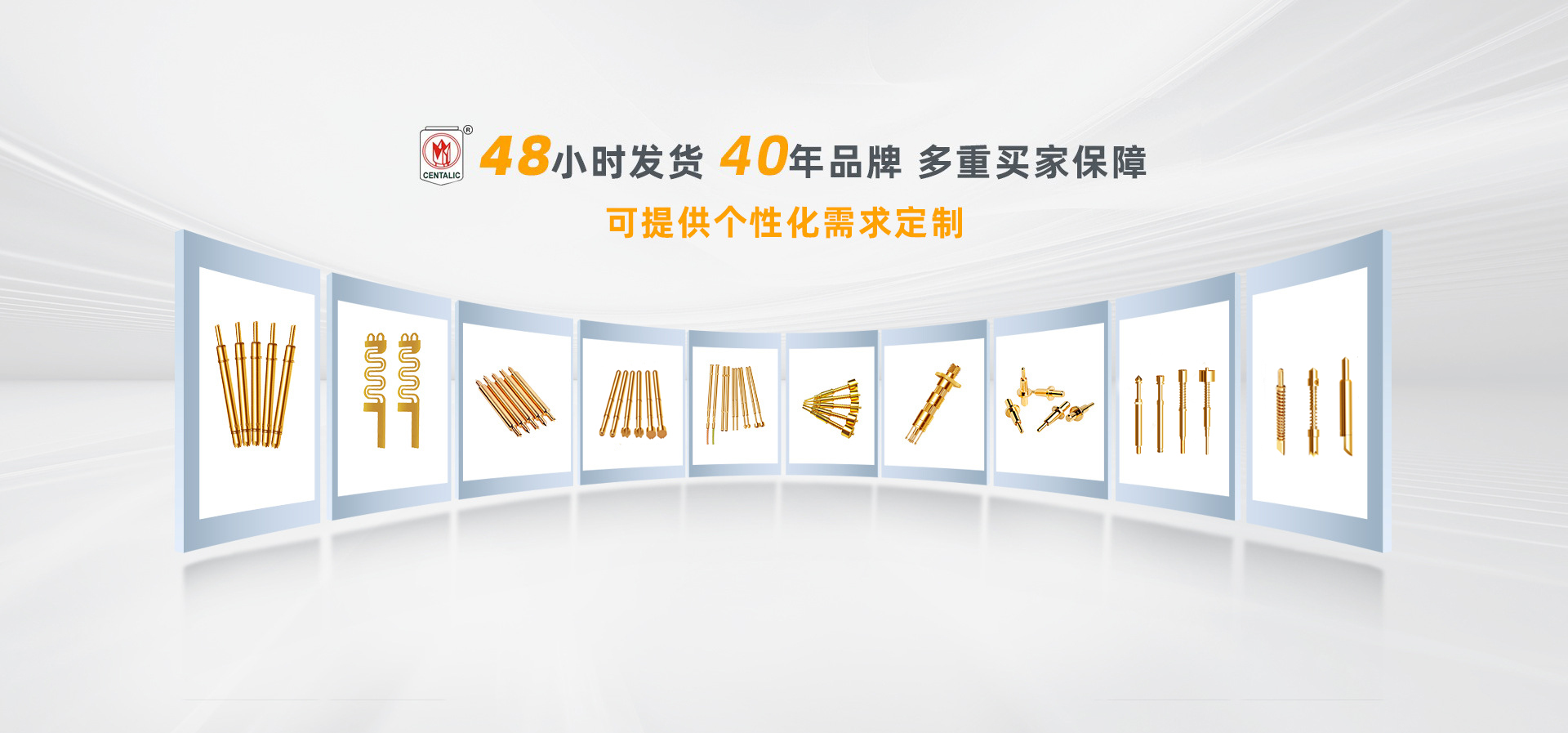
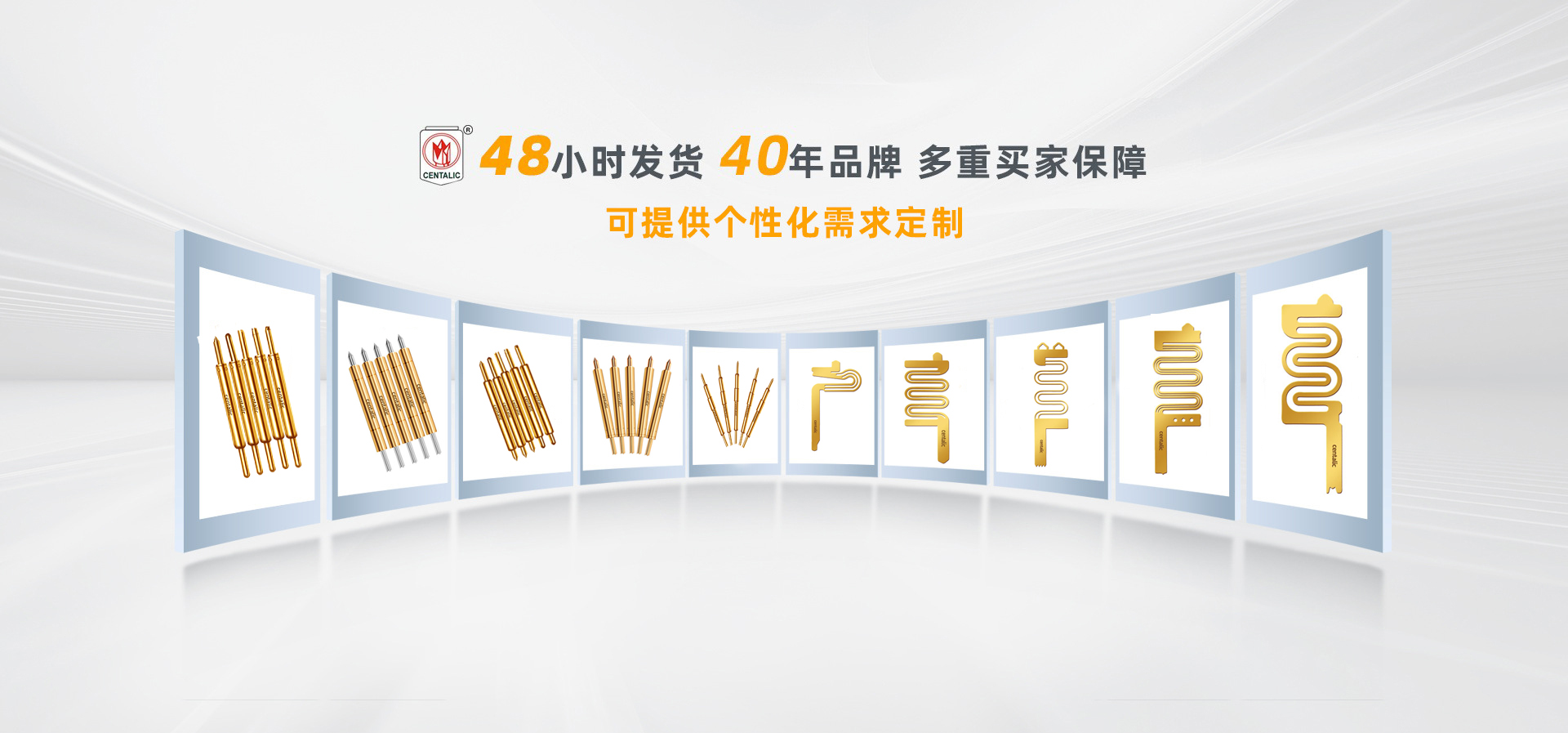
It is mainly composed of three parts: spring, needle tube, and needle tip. According to its structure, it can be divided into two series: double head single action and double head double action. The needle head type can be flexibly selected according to the shape of the test point, and common ones include B-head (pointed) Jhead(Circle) J1head(Small circle) Uhead(Claw) U1head(Claw), etc., to adapt to different pad materials and contact requirements. The typical characteristics of high-frequency needles are small size and extremely high testing accuracy requirements.


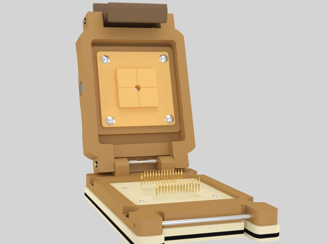
Probes are generally not used independently, but are integrated into a "probe card" or "test stand", playing the role of the core component of the testing component - hence known as the "heart" of the probe card.
At present, Centalic can process high-frequency semiconductor needles with a minimum diameter specification of 0.06mm for the needle tip and 0.10mm for the needle tube, and supports customization based on drawings and samples.
Probes are mainly used for various communication power electronic components, semiconductor wafer testing, chip packaging testing, and other processes. With extremely low contact resistance and ultra-high bandwidth, they can meet the testing requirements of 5-40G high-frequency signals.

AI chips have billions or even billions of transistors, and the pin spacing is constantly shrinking, which puts far more demands on test probes than traditional chips, making probes a "must-have component" for AI chip mass production.

Taking Centalic as an example, its semiconductor high-frequency needle series meets the testing requirements of AI chips in terms of accuracy, performance, and efficiency:
With the evolution of AI chip processes towards 7nm, 5nm, and even 3nm, the pin spacing has been reduced from the traditional 0.5mm to 0.1mmEven smallerThe wafer density has significantly increased. The probe must have extremely high dimensional accuracy to accurately dock each pin in a small space, avoiding offset and signal interference. The precision of the high-frequency needle tip of Suntory Semiconductor has reached the micrometer level, which can meet the requirements of contact accuracy for fine pitch pins.
The high-frequency signals generated in AI chip operations require probes to have ultra-low contact resistance. If the contact resistance is too high, it will cause signal loss and test distortion,In Centalic probe products, the contact resistance is controlled at a low level and has good stabilityEnsure the accuracy and reliability of the test data.
The demand for AI chips in the market has exploded, and mass production efficiency is crucial. The service life and stability of the probe directly determine the testing efficiency. High end probes undergo precision heat treatment and surface treatment, and can withstand hundreds of thousands of insertions and removals. Centalic has optimized the spring design and material heat treatment, which has a long service life, supports large-scale batch testing, reduces downtime and needle replacement costs, and assists in the rapid mass production of chips.
With the evolution of AI chips towards higher computing power and smaller size, and the synchronous upgrading of probes, the industry has ushered in three clear trends.
The probe size continues to break through, the needle diameter evolves towards smaller scales, and tolerance control continues to tighten to adapt to processes of 3nm and below. Synchronized optimization of materials and processes to reduce contact resistance and improve wear resistance.
The global demand for AI computing chip testing is growing rapidly, and the demand for high-end probes and probe cards continues to increase, presenting opportunities for the domestic industry. In the past, high-end probes mainly relied on imports, but now domestic enterprises are increasing their R&D investment and gradually achieving breakthroughs.
In the future, the application of probes will no longer be limited to factory testing, but will extend throughout the entire lifecycle, including design validation, aging testing, and fault diagnosis. For example, during the design validation phase, probes can accurately detect chip design defects and provide data support for optimization.
The small probe, although inconspicuous, is the key gatekeeper for AI chips from design to mass production. With the continuous breakthroughs of domestic probe companies in micro nano processing and material technology, the underlying cornerstone of this "golden track" is becoming more solid. Only by measuring the yield can the starting force be sustained - this probe is worth seeing.