Time:2026-04-03Reading:971Second
In the precision chain of the integrated circuit industry chain, semiconductor probes are essential core components that are easily overlooked by the outside world. It runs through the entire process of chip design verification, wafer manufacturing testing, and packaging testing, serving as a "signal bridge" between chips and testing equipment, directly determining chip yield, testing efficiency, and industry costs. It is the "invisible gatekeeper" of the IC industry from research and development to mass production.
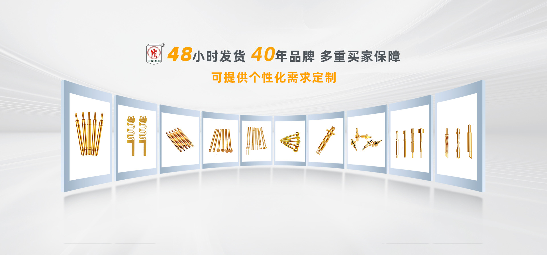
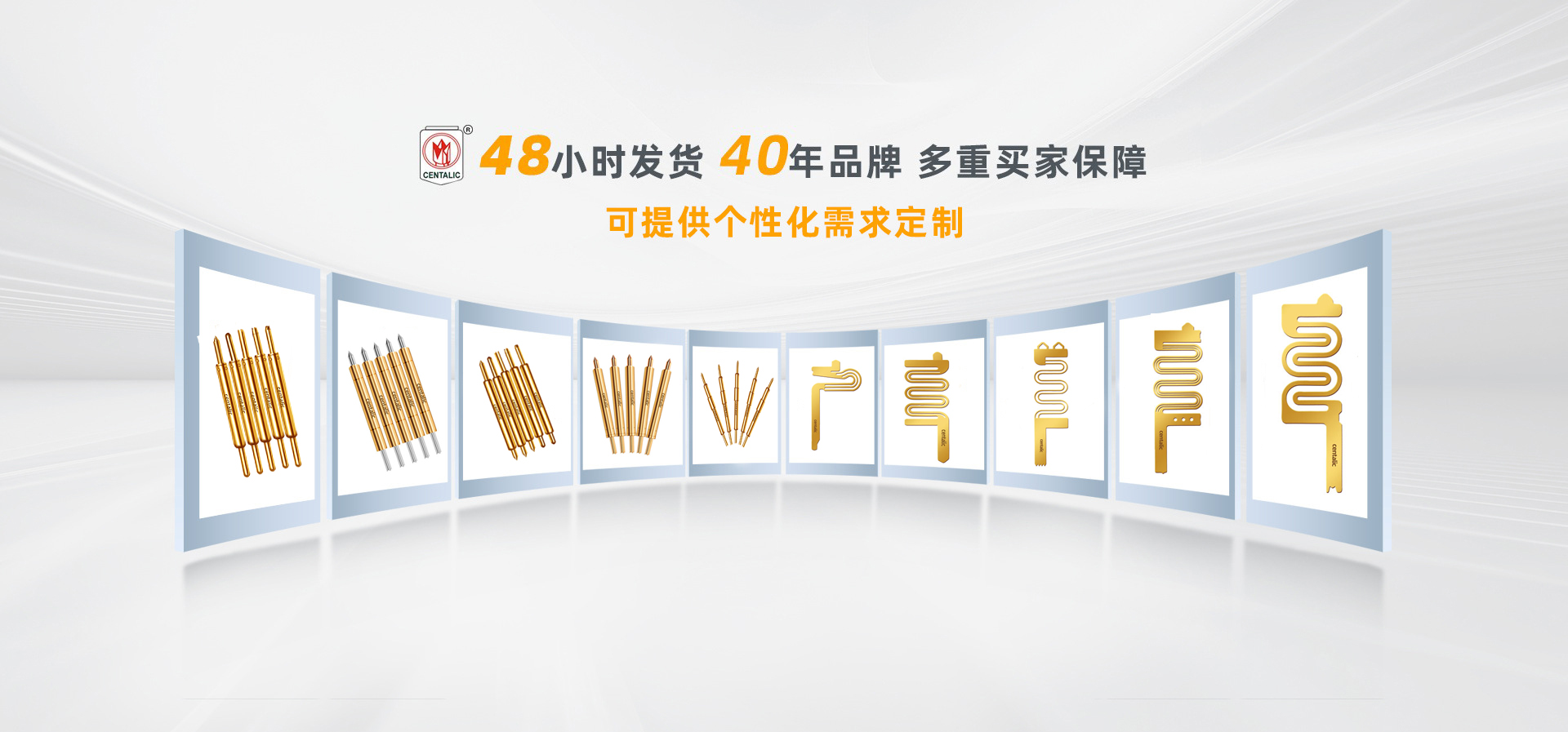
A probe is generally formed by riveting and preloading three basic components: a needle tip, a needle tube, and a spring with precision instruments. Due to the small size of semiconductor products, especially chip products, the size of probes is required to reach the micrometer level, which is a high-end precision electronic component with high manufacturing technology content.

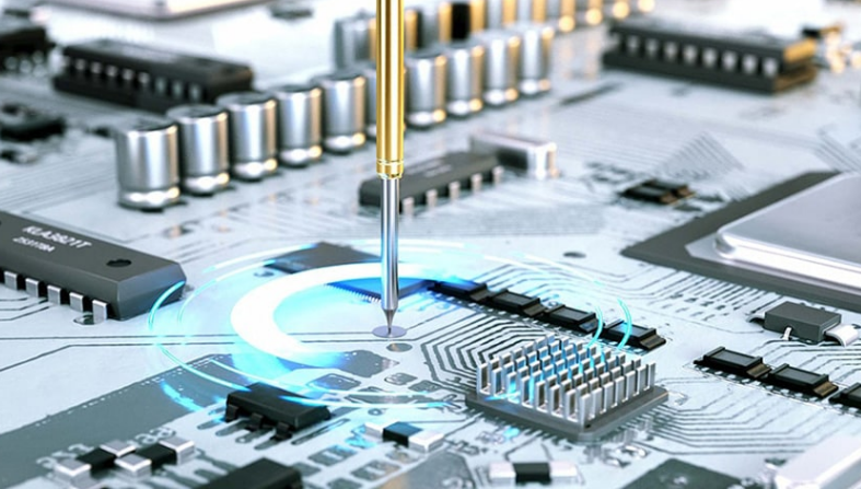
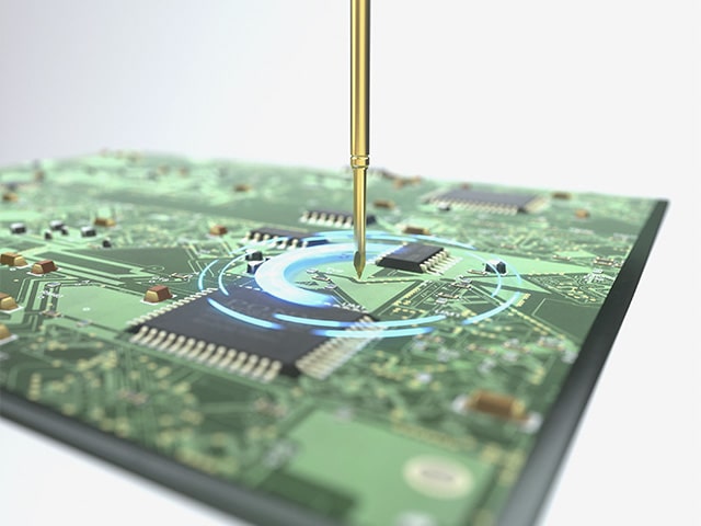
During wafer or chip testing, probes are generally used for precise connection between wafer/chip pins or solder balls and the testing machine, to achieve signal transmission and detect performance indicators such as conductivity, current, functionality, and aging of the product.
The appearance of probes for different purposes varies, but they generally have precise spring structures inside. The surface of the product is generally gold-plated, which has strong corrosion resistance, electrical performance, stability, and durability. As a key component in semiconductor testing equipment, the structure, material, and elasticity of the probe have an impact on its stability and signal transmission accuracy, which in turn affects the testing accuracy of the probe.

From the perspective of the industry chain, probes run through the entire process of semiconductor product design, manufacturing, packaging testing, and application, mainly covering three key stages:
Design verification phase:After the chip design is completed, probes are used to verify whether the functionality of the chip design meets expectations, helping designers identify problems and optimize the design before chip fabrication.
Wafer testing:Before chip cutting and packaging, a "probe card" carrying hundreds to thousands of probes simultaneously conducts contact testing on the entire chip on the wafer. This stage is like "prenatal screening", quickly screening out defective products to avoid them flowing into high cost packaging processes, which directly affects manufacturing costs and efficiency.
Finished product testing:After the chip is packaged, the probe conducts comprehensive functional and performance verification of individual chips in the testing socket. This is the "final physical examination" before delivery to ensure that each factory chip meets the design specifications and can work stably in real applications.

A high-end chip requires thousands of probe contacts, and the accuracy, stability, and durability of the probes themselves directly determine the accuracy of testing yield and the final quality of the product.
Centalic was established in 1992 as a wholly-owned subsidiary of Hong Kong Centalic Technology Development Co., Ltd. It is a national high-tech enterprise that integrates research and development, production, sales, and technical services. It is one of the earliest enterprises in China engaged in large-scale and professional production of various testing probes and precision hardware products. The company has introduced advanced production and inspection equipment from both domestic and foreign sources, implementing a "one-stop" production management model from product technology research and development, raw material and production processing, to finished product sales. It fully and efficiently cooperates with customers to develop probes for testing projects.
In terms of technical parameters, Centalic can process semiconductor probes with a minimum needle diameter of 0.06 mm and a needle tube diameter of 0.10 mm. Its semiconductor probe has extremely low contact resistance and ultra-high bandwidth, which can meet the testing requirements of 5-40G high-frequency signals. Covering various testing scenarios from consumer electronics to 5G communication chips.
In terms of product matrix, Suntory has built a probe solution system covering the entire semiconductor industry chain. Its core products include: a series of semiconductor test pins for wafer testing and chip packaging testing; ICT test needle series for online circuit testing; High current needle series for high-temperature and high current scenarios; Bullet pin series for precision spacing connector testing; Kelvin needle series for micro resistance testing; As well as RF needles, non-magnetic probes, PCB spring needles, charging needles, etc., they are widely used in various fields such as semiconductor chips, mobile phone screen modules, automotive electronics, medical equipment, aerospace and military industry, new energy, smart home wearables, etc.
Currently, semiconductor probe technology is rapidly evolving towards higher precision, stronger performance, and wider application scenarios. At the technical level, the industry presents three significant trends:
Higher precision and microfabrication:As the chip process evolves towards 2nm and more advanced nodes, the size of chip pads has been reduced to below 50 microns, and probes need to achieve precise contact in less than 100 microns of space.
Higher frequency and signal integrityEmerging applications such as 5G/6G communication, AI computing chips, and autonomous driving have raised higher requirements for high-frequency signal testing, and impedance matching and loss control of probes have become key technical challenges.
Longer lifespan and high reliabilityTesting probes need to withstand tens of thousands or even hundreds of thousands of repeated contacts without failure, and surface gold plating technology, fatigue performance of spring materials, and needle tip wear resistance have become the core indicators for measuring quality.
Although semiconductor testing probes are small in size, they are the "invisible gatekeepers" that run through the entire process of the IC industry chain. From design verification to wafer testing to finished product testing, it ensures the yield and reliability of each chip with micrometer level precision connections, directly affecting the cost efficiency and technological progress of the entire semiconductor industry.