Time:2026-06-24Reading:948Second
It is as thin as a hair, but it can carry signals from thousands of troops and horses. It is as light as a feather, yet it can accurately "pinpoint" on the battlefield at the micrometer level.
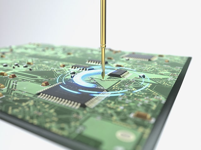
This is the probe. An inconspicuous metal needle, with its extremely small body, has conquered precision testing fields from semiconductor wafers to consumer electronics, from automotive electronics to aerospace.
Although probes are small, they come in a wide variety of categories. Different application scenarios correspond to different probes. Common probe types include:
1. Semiconductor probes - series:
Mainly used for various communication power electronic components, semiconductor wafer testing, chip packaging testing, etc., with extremely low contact resistance and ultra-high bandwidth, it can meet the requirements of 5-40G high-frequency signal testing. At present, for this series of probes, Suntory can process the minimum probe diameter: needle diameter: 0.06mm/needle tube diameter: 0.10mm.

2. High current probes - series:
Mainly used in the field of online testing for high temperature and high current. Its characteristics are high testing current and high testing temperature conditions.

3. ICT Probe Series:
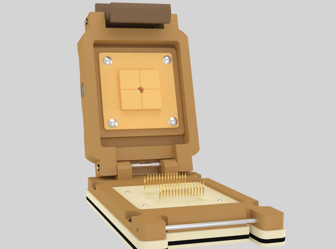
Mainly used for online circuit testing and functional testing, detecting the electrical performance of online components on the board and the connection status of the circuit network, and being able to quantitatively measure and perform functional testing on the components. Usually, ICT online testing needles are used together with their matching size needle sleeves, which are fixed on the PCB board for easy replacement of probes at any time.

4. Kelvin Probe Series:
Mainly used in the field of resistance testing, it is suitable for testing electronic components with small and low resistance values.

5. RF Probe - Series:
Mainly used for signal insertion, detection, and measurement output of high-frequency RF, RF, and microwave modules, as well as electrical performance analysis of high-frequency circuit boards. Having the characteristics of relatively concentrated signals that can pass through and low loss, there are very high requirements for the impedance and loss of RF probes in the testing of high-speed digital circuit boards and microwave chips. The design structure of RF probes is complex, with multiple components and high added value, and they are mostly customized.

6. Bullet Probe - Series:
Mainly used for testing precision spacing connectors such as mobile phones, chips, screens, etc. It has the characteristics of being able to handle smaller pitches, high testing efficiency, high stability, and long lifespan, and plays a role in transmitting signals and conducting currents.

7. Non magnetic probes - series:
Made of non-magnetic materials, mainly used for areas that are difficult for inspectors to directly inspect. It can meet the testing requirements in special non-magnetic environments, such as the inspection of medical devices, underground or stored goods, and improve the safety factor during inspections in dangerous and difficult environments. It has been widely applied in multiple fields.

How small is the smallest probe? The diameter of ordinary adult hair strands is about 0.07mm, whileThe minimum needle size of the Suntory semiconductor probe is only 0.06mm, which is finer than a hair.
The small test probe carries the quality bottom line of the entire electronics industry. Between square inches and micrometers, with its precision and stability, it has become an indispensable core cornerstone of precision manufacturing. Centalic has a profound understanding of this: every probe that leaves the factory must go through the entire process from raw material input, turning processing, cleaning, heat treatment, electroplating, assembly, inspection and shipment, with strict control over each process. Only in this way can we ensure that it can withstand, measure accurately, and last for a long time in the customer testing position.

The conquering power of probes lies not only in their ultimate precision, but also in their powerful adaptability - they are not limited to a single field, but have conquered one professional testing scenario after another with flexible structural design and diverse parameter configuration, becoming an indispensable core testing device in multiple industries.
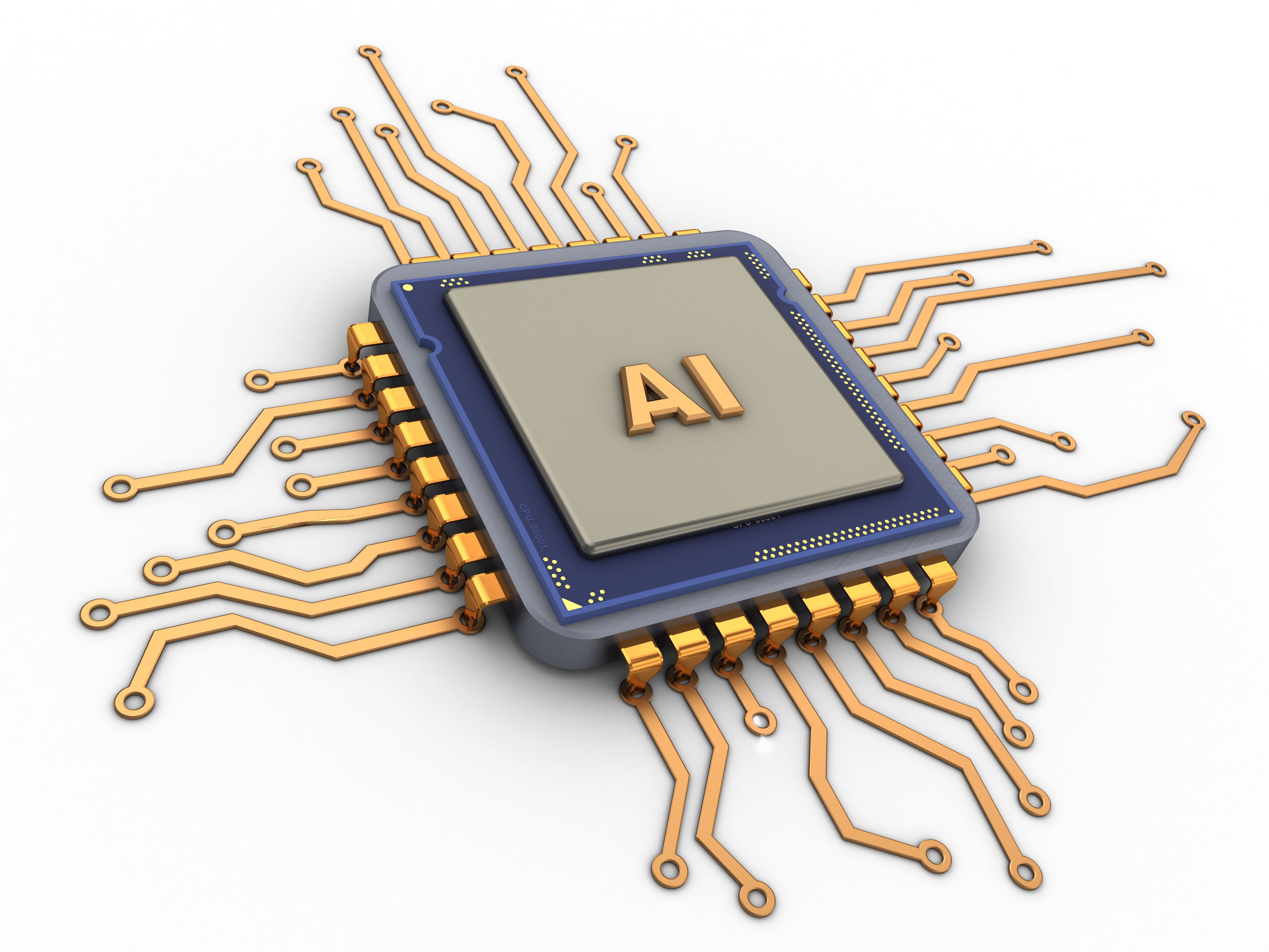
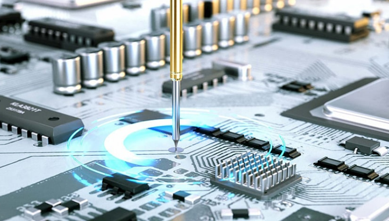
In the semiconductor industry chain, probes are the "quality guardians" that run through the entire process of wafer testing and chip packaging testing. Whether it is high-end computing chips such as AI chips, CPUs, GPUs, or ordinary consumer electronics chips, every chip from design blueprints to mass production cannot do without precise calibration of probes. It is connected to the pins and solder balls of the chip on one end, and to the testing equipment on the other end, like a "microscopic stethoscope", capturing every performance signal of the chip at the micrometer scale, detecting the conductivity, current stability, and functional integrity of the chip, and even simulating the aging performance under extreme working conditions such as high temperature and high frequency, screening out unqualified products, and providing core data support for chip design optimization and mass production landing.
In the field of medical equipment testing, probes can accurately detect the circuit conductivity and signal transmission stability of medical instruments, ensuring the safety and reliability of medical equipment in clinical applications, and guarding the human health defense line with a small body.
In the field of new energy,Probes are widely used for performance testing of power batteries and photovoltaic modules.Accurately detect the stability of power battery voltage and current transmission, and identify internal circuit hazards; Docking with micro contacts of photovoltaic cells, verifying the photoelectric conversion efficiency, and assisting in the safety upgrade and performance optimization of new energy products.In the aerospace field, probes have conquered harsh testing scenarios such as high and low temperatures with their excellent resistance to extreme environments.
In addition to the core areas mentioned above, probes are also present in multiple fields such as electronic manufacturing. In the field of electronic manufacturing, it is used for on/off testing of PCB boards and electronic components to ensure the circuit stability of products.
Regardless of the field, the probe always completes its mission with its "small yet powerful" body.
Probes can conquer vast testing fields without continuous iteration and upgrading of technology. From traditional single head probes to dual head probes with bidirectional adaptation, from conventional materials to materials that are resistant to high temperatures, corrosion, and low contact impedance, from single scene adaptation to multi domain universality, every upgrade of the probe gives its "small body" stronger "conquering power" to meet increasingly complex and high-end testing needs.
In the wave of technological iteration, two major trends are particularly evident:
One is the continuous improvement of accuracy,The size of the probe continues to shrink, and the diameter of the needle breaks through to smaller sizes, further tightening the tolerance control; The material and process are continuously optimized to further reduce contact resistance, improve wear resistance and oxidation resistance.
The second is the acceleration of localization substitution,Previously, high-end probes mainly relied on imports, but with the rise of domestic semiconductor, medical and other industries, domestic enterprises have continuously increased their R&D investment, allowing domestic probes to conquer more domestic and even global markets with high cost-effectiveness and high adaptability.
It doesn't have a grand volume, but it can leverage the development of the entire precision manufacturing industry; It may seem ordinary and unremarkable, but it carries the quality mission of every product. Probes, with their small bodies, have conquered vast testing fields and silently played the roles of "micro messengers" and "quality guardians" in multiple industries such as semiconductors, healthcare, new energy, and aerospace.
In Centalic's view, the mission of each probe is not just about "contact", but precision, reliability, and durability. From raw materials to finished products, every process follows strict standards; From conventional shelf products to deep customization solutions, every delivery is a commitment to customer testing responsibility.
Every precise strike is a strict control of quality; Every signal transmission is a pursuit of technology. With the continuous development of technology, the requirements in the testing field will become more stringent, and probes will continue to iterate towards finer, more accurate, more durable, and more diverse directions. It will continue to conquer a wider testing world with its small body, break through one technological barrier after another, safeguard technological progress and industrial upgrading, and write a legend of "great power" belonging to the micro world.