Time:2026-05-13Reading:889Second
Today, as the semiconductor industry accelerates its penetration into advanced processes and high reliability scenarios, chip aging testing has shifted from an "optional link" to a "must pass checkpoint". It accelerates stress through high temperature, high pressure, and long-term electrification, exposing potential defects in the chip in advance, and is the core barrier to ensure long-term stable operation of the chip. But with the soaring integration of chips, miniaturization of process nodes, and strict testing standards, the "pain points" of aging testing are becoming increasingly prominentSemiconductor probeIt is the key answer to solving these difficult problems.
Chip aging testing is the process of comprehensively testing and evaluating chips by simulating actual working conditions under long-term use and various extreme environments. Its goal is to verify the stability and reliability of the chip under long-term use and extreme conditions. However, this testing process faces many challenges:
● High testing complexity:With the continuous improvement of chip integration, the complexity and difficulty of aging testing are also increasing. Testers need to simulate various environmental factors, such as high temperature, low temperature, high humidity, etc., to verify the stability of the chip in different environments.
Long testing time:Aging testing requires long-term operation to evaluate the lifespan and performance degradation of the chip. This not only consumes a lot of time and resources, but also places extremely high demands on testing equipment and environment.
High testing accuracy requirements:To ensure the accuracy of test results, aging testing requires high-precision testing equipment and probes. Any small error can lead to deviation in test results, thereby affecting the assessment of chip performance.

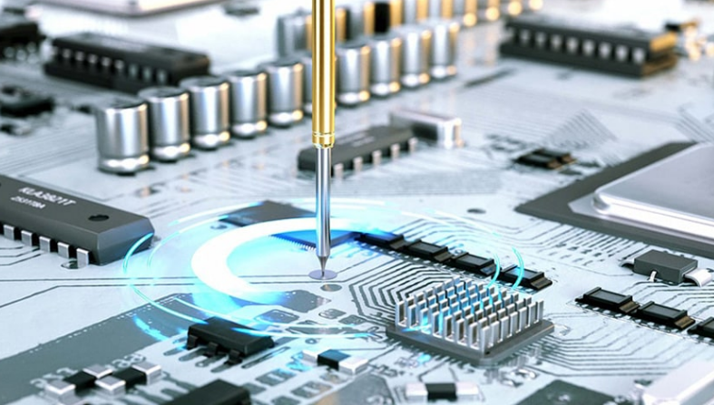
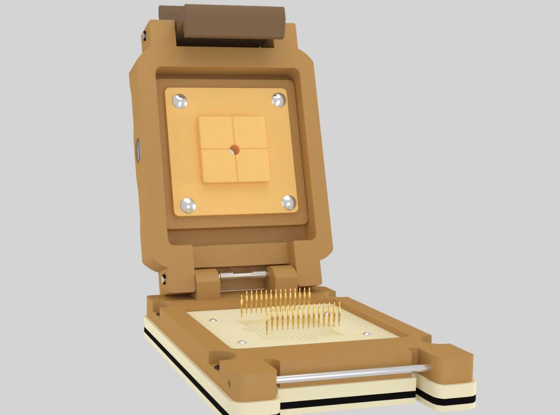
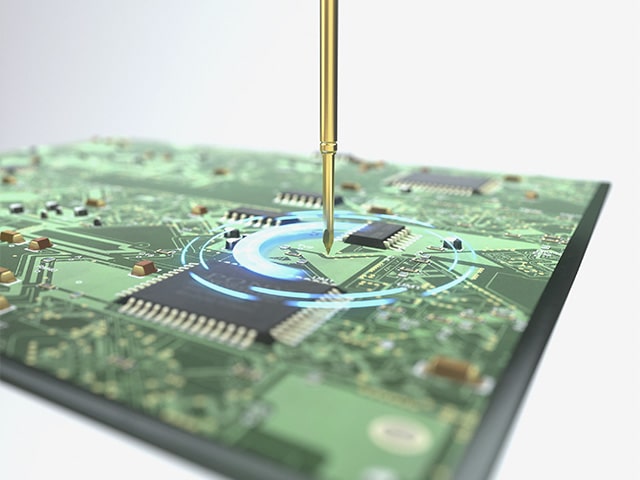
Faced with the many challenges of chip aging testing, a high-performance semiconductor probe has become the key to breaking through. Semiconductor probe, also known as dual head probe,itsThe function is to make contact with the chip through tiny probes after the chip manufacturing is completedEstablish physical connections, transmit test signals to the interior of the chip, and read feedback data.
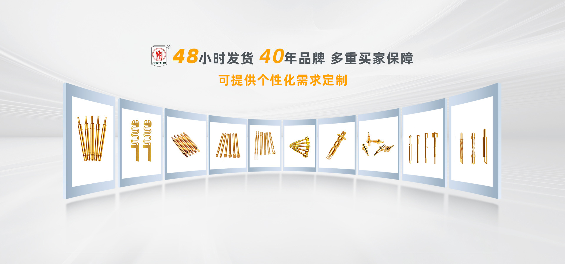
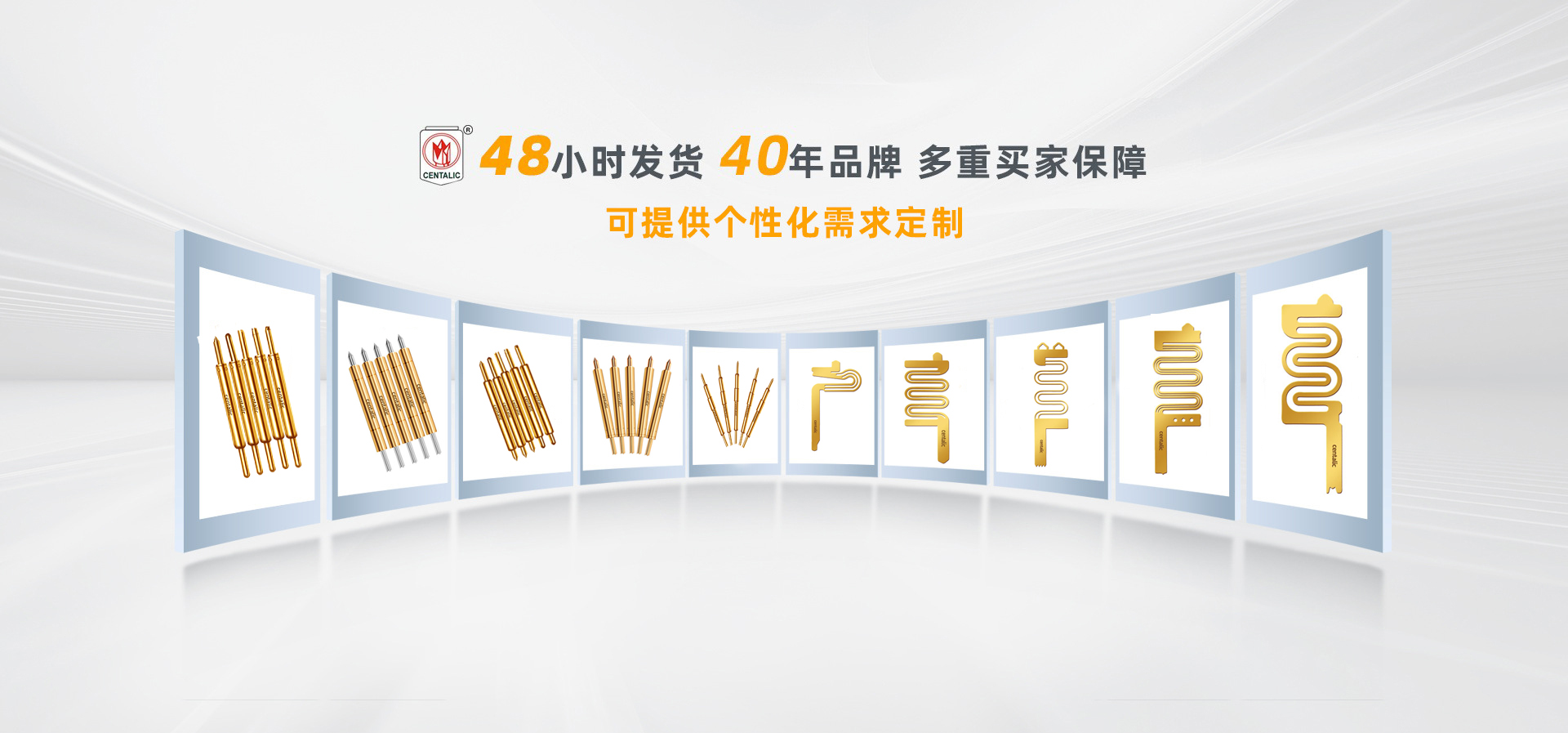
As a national high-tech enterprise with a "fully self operated large-scale" probe production line, Centalic has been focusing on the research and manufacturing of various testing probes for more than 40 years.Can provide processing capabilities in the field of semiconductor probes——The minimum needle diameter can reach 0.06mm and the needle tube diameter can reach 0.10mm, providing a solid hardware foundation for high-density aging testing.The semiconductor probe designed specifically for aging testing has the following core advantages:

1. Temperature resistant and manufacturing resistant, stabilizing the "contact lifeline" in extreme environments
High temperature during aging testinglow temperatureIt's ordinaryprobeof'Nightmare'.High quality aging testingProbe adoptsBeryllium copper gold platingHigh-temperature resistant springmaterialHas excellent adaptability to a wide temperature range and can withstand harsh conditionsenvironmentStill able to withstand impactmaintainLow and stable contact resistance, long-term use without drift, oxidation, or false connection, ensuring uninterrupted signal throughout hundreds of hours of testing.
2.Long lifespan and durability, able to withstand the pressure of mass production testing
Aging testing not only takes a long time per test, but also requires tens of thousands of insertions and removals of probes during mass production. Equipped with high-precision springs, it has an ultra long mechanical dynamic life at room temperature; In high temperature environments, stable contact force can still be maintained for a long time with extremely low attenuation of elasticity. This significantly reduces the frequency of probe replacement and significantly lowers production line downtime costs.
Imagine what would happen if low-quality probes were used in the aging test?
Contact resistance drift at high temperatures leads to the invalidation of long-term test data, resulting in a significant waste of production capacity;
Probe elasticity attenuation or offset, misjudging good products, and high-quality chips being mistakenly scrapped;
The lifespan of the probe is insufficient, the production line frequently stops for replacement, and the delivery cycle is infinitely extended.
The accuracy, stability, and durability of semiconductor probes directly determine the success or failure of aging testing, which in turn affects the reliability and market competitiveness of chips.
Chip aging testing is a necessary path for the semiconductor industry in the era of "quality is king"; ButSemiconductor probes designed specifically for agingIt is the 'optimal solution' to overcome its core pain points. It is not only a "signal bridge" connecting chips and testing equipment, but also a "solid foundation" to resist extreme environments and ensure testing stability.
In the current era of accelerated iteration of advanced processes and continuous upgrading of reliability requirements,First profitWith over 40 years of technological accumulation, fully self operated production lines, and continuously optimized probe performance, we provide stable and reliable solutions for chip aging testing. Centalic is committed to making every probe an important node in the reliability management of the entire life cycle of chips, helping the semiconductor industry overcome reliability difficulties and move towards higher quality development.