Time:2026-03-13Reading:1116Second
In the precision microscopic kingdom of semiconductor manufacturing, when chips are completed on a wafer“birth”When preparing for the test, a low-key yet crucial character will appear——It is a semiconductor testing needle. It's like a“medical examiner”Accurately touch each chip and perceive their“pulse”and“heartbeat”Select qualified products. So, this one“doctor”What exactly does it look like? How small is it really? Why is it so important?

Semiconductor test needle, also known as double headedProbe is a high-end precision electronic component and a key core component in wafer and chip testing.
Divided by structure: double head single action probe, double head double action probe series.
Mainly used inVarious communication power electronic components, semiconductor wafer testing, chip packaging testing and other processes, with extremely low contact resistance and ultra-high bandwidth, can meet the requirements of 5-40G high-frequency signal testing.
Its main job is to act as a bridge between the chip and the testing equipment in the wafer testing and finished product testing stages of the chip“Signal bridge”.

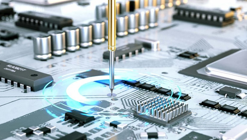
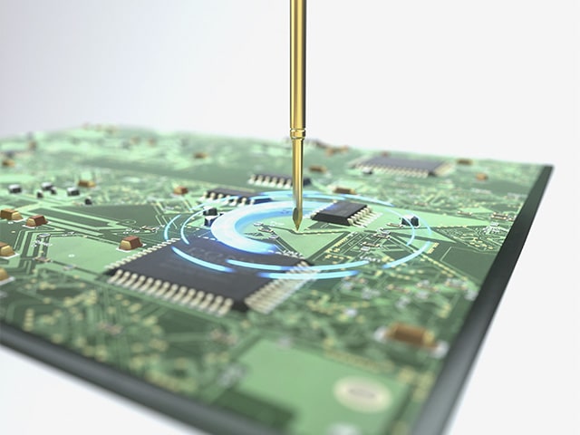
You can imagine it as a precision electronic component thinner than a strand of hair. During testing, the head of the test needle will make precise contact with the tiny pins or solder pads of the chip, while the other end is connected to the testing instrument. Through this probe, current and signals can be transmitted between the chip and the device, thereby detecting the electrical performance and functionality of the chip, and ultimately screening out products with design or manufacturing defects. This process is crucial for ensuring product yield and controlling production costs.
test probeof“small”This is mainly reflected in two aspects:
Small diameterThe diameter of semiconductor probes is usually a few millimeters, much thinner than the tips we use in our daily lives.This type of semiconductor probe can first be processed with a needle diameter of φ0.06mmNeedle tube0.1mm,Equivalent to the thickness of a strand of hair..
Short in lengthThe length of the test needle is generally only a few millimeters. In some testing scenarios that require high-density layout, the probe spacing is compressed to the extreme, and the requirements for manufacturing accuracy also reach the micrometer level.

Taking semiconductor probes as an example, their internal structure is as precise as a miniature mechanical artwork.
threeMajor core components:It usually consists of three basic parts: needle, needle tube, and spring.
syringe needle:This is the part where the probe comes into direct contact with the chip,For different testing points, there are various head types to choose from for the needle, such as pointed or round headVarious head types, including claw heads,To adapt to diverse testing needs..
Needle tube:Provide mechanical support and signal transmission channels. Internally equipped with springs,To ensure the stability and reliability of contact pressure during testing.
Spring:This is a probe“heart”A precise spiral coil. When the needle is compressed, the spring is compressed, providing stable elastic contact force, ensuring that the needle and the chip are always tightly attached, while buffering mechanical impact and protecting the chip from being crushed.

Working Principle:When the test begins, the test needle will move along with the probe station, accurately aligning with the pins of the chip. Then, a slight pressure is applied downwards by the probe, causing the needle to retract and the internal spring to be compressed, resulting in a stable and controllable contact force. In this way, the electrical circuit is established, and the test signal can be smoothly transmitted bidirectionally between the chip and the testing equipment through the test pin.
It can be said that without test needles, there would be no mass production of modern chips. Its importance is reflected in the following aspects:
The quality of chips“gatekeeper”:The test needle is the last checkpoint before the chip leaves the factory. It works in conjunction with testing systems to accurately identify defective chips, preventing them from entering the market and affecting the reliability of end products.
Control intoThe key to this:In semiconductor manufacturing, the earlier defects are discovered, the greater the cost of recovery. Screening out defective chips with testing needles during the wafer stage can avoid expensive packaging for these defective chips in the future, greatly saving costs.
Supporters of technological iteration:With the continuous improvement of chip manufacturing processes and the increasing density of pins, the testing frequency continues to rise, and the requirements for testing pins also rise accordingly. To meet the testing requirements of the new generation of communication chips, the testing needle needs to support high-frequency signal transmission; To cope with power chips in fields such as new energy vehicles, a single probe needs to have stronger high current carrying capacity. Every breakthrough in testing needle technology provides solid support for the iterative development of high-performance chips.
In summary, although semiconductor probes are small, they serve as a link between microscopic chips and the macroscopic world“Key touch”.From birth to transformation, every chip cannot do without this precise "examination" before possessing powerful "intelligence".It is the reliable contact of the testing needle that supports the towering structure of the modern electronic information industry.
And Centalic is one of the silent builders of this pedestal. Having been deeply involved in the field of probes for forty years, Suntory has a fully self operated large-scale production line, which is complete and perfected“one-stop service”Production line. After receiving raw materials, turning processing is carried outCleaning, heat treatment, electroplating, assembly, inspection and shipment are all controlled by our company's self operated production line, with standardized production processes and strict control over delivery time and quality. This not only ensures product consistency and reliability, but also enables Suntory to quickly respond to customers' personalized needs, providing one-stop probe customization solutions from standard testing probes to special application scenarios.