Time:2025-12-12Reading:1514Second
With the rapid development of semiconductor technology, chips, as the core carrier of information technology, have become the key to promoting technological progress by improving their performance and quality. However, chips inevitably experience aging during long-term use, which directly affects the performance and lifespan of electronic products. Therefore, chip aging testing has become a crucial link in the semiconductor industry. This article will delve into the challenges faced by chip aging testing and introduce a semiconductor high-frequency needle that can easily break through.

Chip aging testing is the process of comprehensively testing and evaluating chips by simulating actual working conditions under long-term use and various extreme environments. Its goal is to verify the stability and reliability of the chip under long-term use and extreme conditions. However, this testing process faces many challenges:
High testing complexity: With the continuous improvement of chip integration, the complexity and difficulty of aging testing are also increasing. Testers need to simulate various environmental factors, such as high temperature, low temperature, high humidity, etc., to verify the stability of the chip in different environments.
Long testing time: Aging testing requires a long period of operation to evaluate the lifespan and performance degradation of the chip. This not only consumes a lot of time and resources, but also places extremely high demands on testing equipment and environment.
High testing accuracy requirements: In order to ensure the accuracy of test results, aging testing requires high-precision testing equipment and probes. Any small error can lead to deviation in test results, thereby affecting the assessment of chip performance.

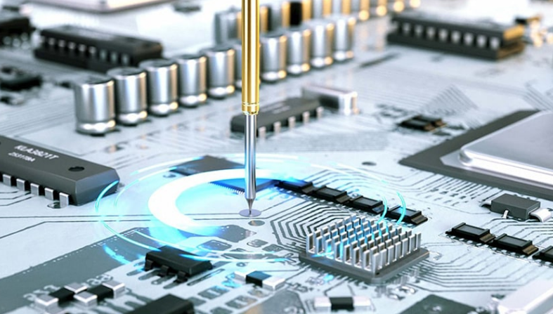
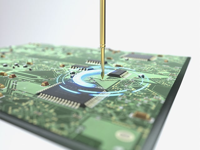
Faced with the many challenges of chip aging testing, a high-performance semiconductor high-frequency needle has become the key to breaking through.Semiconductor high-frequency probe, also known as dual head probe, is used to physically connect with the contact points of the chip through tiny probes after the chip manufacturing is completed,Connect one end to a chip pin (or wafer solder ball) and the other end to a testing machine to accurately transmit electrical signals, detect the conductivity, current stability, functional integrity, and even aging performance of the chip in high temperature environments.

halfconductorHigh frequency needleThe advantage lies in "high precision and strong adaptability", with extremely low contact resistance, ultra-high bandwidth, and support for 5-40G high-frequency signal transmission testing requirementsTo meet the testing needs of multiple stages such as communication power electronic components, semiconductor wafer testing, chip packaging testing, etc.
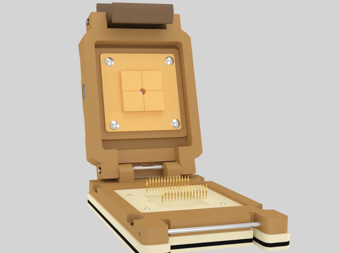
Centalic is a national high-tech enterprise with over 40 years of "fully self operated and large-scale" probe production lines, focusing on the research and manufacturing of various testing probes. Mainly producing various types of testing probes, providingOne stop testing plan andProbe customization service! This type of semiconductor high-frequency needleMinimum probe diameter that can be processed: needle diameter: 0.06mm/needle tube diameter: 0.10mm.
Against the backdrop of chips moving towards more advanced processes, increasing integration and complexity, aging testing is no longer an optional process at the end of the manufacturing process, but a crucial path to ensure product reliability, brand reputation and safety. Semiconductor high-frequency needles, as the ultimate bridge connecting the physical world and electrical testing, every micron level improvement in their performance and every breakthrough in materials science directly translates into deeper and more accurate insights into chip lifespan and reliability.
It is not onlyThe weapon to solve the dilemma is an indispensable precision gear in the quality foundation of the semiconductor industry. In the future, as chips enter a new era of three-dimensional integration and heterogeneous integration, the requirements for test probes will become increasingly stringent, and their technological innovations will continue to resonate with the evolution of chip technology, safeguarding the stable operation of every chip over the long years.