Time:2025-11-22Reading:1359Second
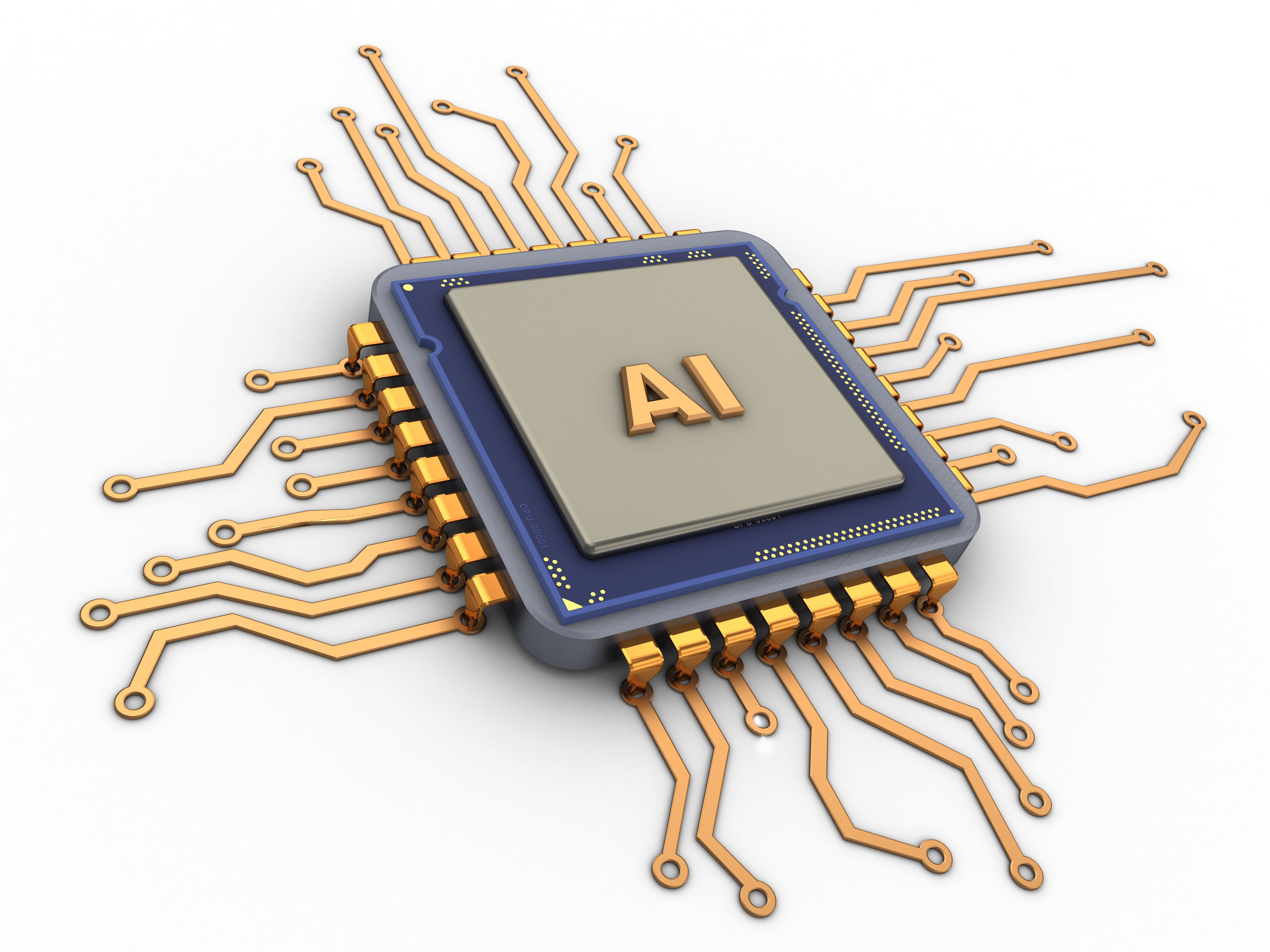
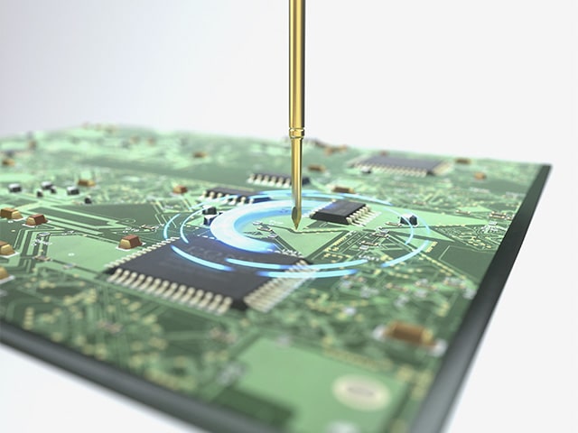
As AI big models, autonomous driving, and computing power clusters become high-frequency buzzwords in the technology industry, the golden track of AI chips is expanding at an astonishing speed. However, every high-performance AI chip, from its design blueprint to practical application, cannot do without a key "quality inspection pass" - the precise calibration of semiconductor testing probes. These seemingly tiny precision devices, like the "microscopic stethoscope" of the chip industry, safeguard the performance and reliability of chips with high precision, becoming an indispensable core support behind the rise of the AI chip race.
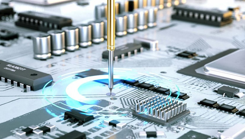
Before the chip is cut and packaged, thousands or even tens of thousands of probes on the test probe card need to make precise contact with the tiny solder pads of each chip on the wafer. During this process, the probe needs to:
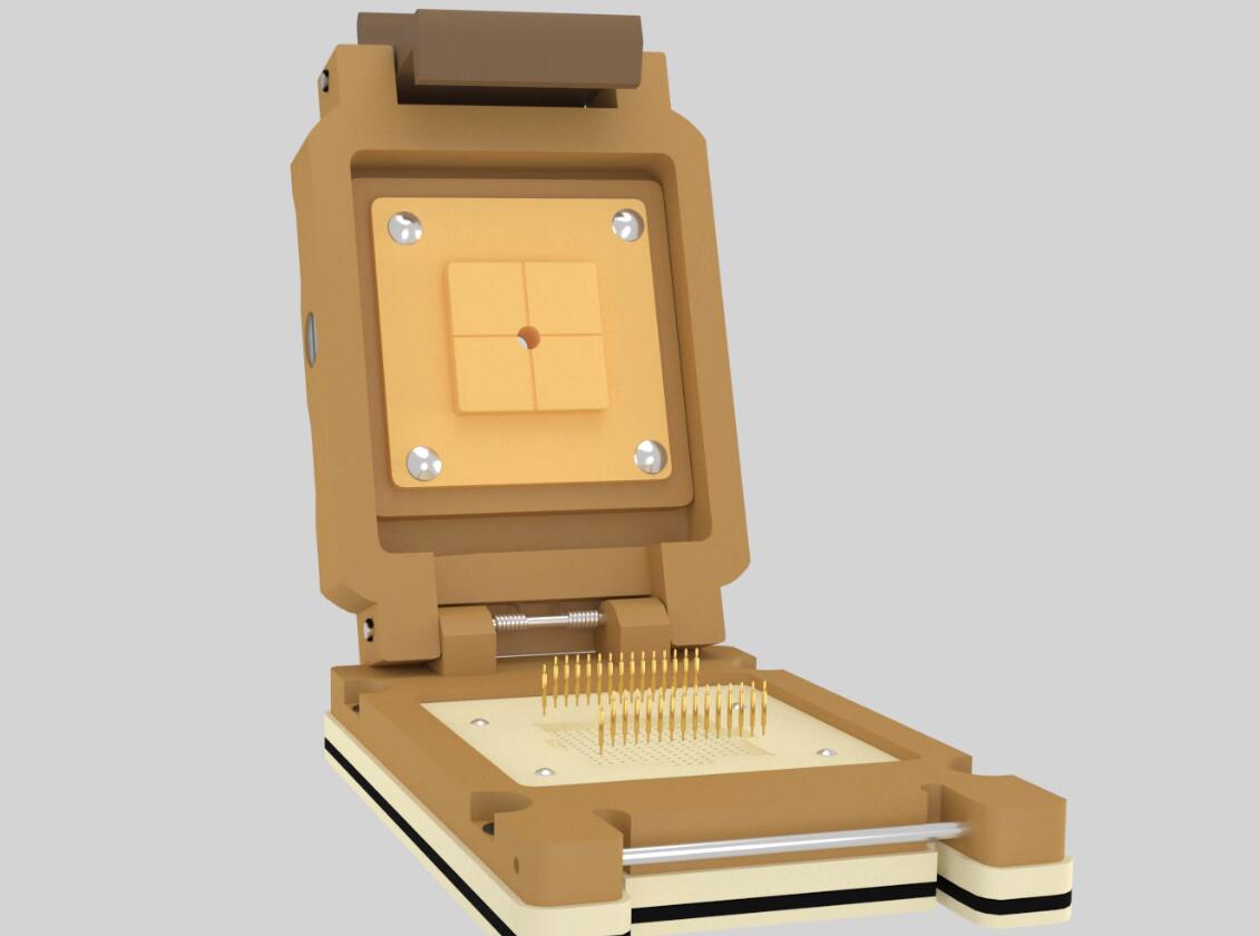
After the chip packaging is completed, test the socket(Socket)The probe inside will once again make contact with the pins or solder balls of the chip for the final comprehensive test“physical examination”At this point, the probe needs to:
The "particularity" of AI chips has transformed the semiconductor testing process from a "conventional process" to an "extreme challenge", and probes, as the "first checkpoint" of testing, are the first to face three major changes:
1. Pin count explosion: Density revolution drives technological iteration
The pin count of ordinary chips is usually in the tens to hundreds, while AI chips, due to high integration, have skyrocketed to thousands of pins. This means that the probe card needs to accommodate more probes, with smaller spacing and higher precision requirements for the probes. Any slight deviation can lead to test failure.
2. Increased testing phase: Durability becomes a key indicator
To cover potential defects in AI chips, advanced processes below 7nm must add two new testing steps to directly test the performance limits of probes:
To cover potential defects in AI chips, advanced processes below 7nm must add two new testing steps:
System level testing:Simulate the actual working scenario of the chip, requiring the probe to transmit signals stably for a long time;
Three temperature aging test:Tested at extreme temperatures ranging from -40 ℃ to 125 ℃, the probe material must be resistant to high and low temperatures;
These two major links not only accelerate the wear and tear of probes, but also drive the unit price of high-end probes from "a few dollars/piece" to "tens of dollars/piece", directly driving market growth.
3. Advanced Process Packaging: Challenging the Limit of "Refinement"
With the evolution of AI chips towards 5nm and 3nm processes, as well as the popularity of advanced Chiplet packaging, the testing nodes of chips are becoming smaller, which requires probes with smaller tip diameters and higher testing efficiency.
As AI computing power grows 1000 times every 8 years and 3nm and 2nm processes gradually land, the growth logic of the probe market is shifting from "short-term demand explosion" to "long-term technology driven". In the future, probes will continue to evolve towards finer details, higher frequencies, and greater resistance to extreme environments.
In this "computing power competition" of AI chips, although semiconductor test probes are located at the back end of the industry chain, they are directly related to whether the chip can move from the laboratory to the highway of mass production. With the continuous breakthrough of domestic technology, Chinese enterprises are accelerating their pursuit with "precision on the needle tip". When every AI chip runs stably under the precise calibration of probes, we are one step closer to the imagined era of general artificial intelligence.