
Time:2026-10-21Reading:841Second
Have you ever noticed a detail:
For traditional mobile phone processor testing, a few hundred needles on the probe card are sufficient. But in the generation of AI training chips, a probe card can easily have thousands or tens of thousands of test probes, and the industry's "tens of thousands of probes tested together" is no longer news.
Many people's first reaction is: Is it a waste of design? Can you use it less?
It's not a waste. AI chips are being forced out by several trends in hard physics. Today, puncture this layer of window paper.
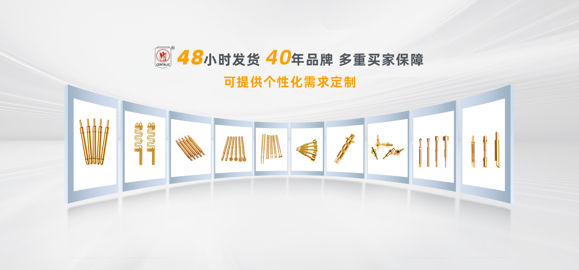
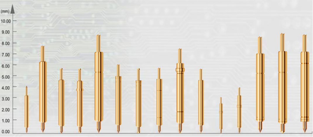
AI chip testing generally uses semiconductor testing needles, also known as double headed probes. Probes are generally composed of three parts: needle tip, needle tube, and spring. According to their structure, they can be divided into two series: double headed single action and double headed double action. The needle head type can be flexibly selected according to the shape of the test point. Common types include B-head (tip), J-head (circle), J1 head (small circle), U-head (claw), U1 head (small claw), etc., to adapt to different pad materials and contact requirements. The characteristics of dual head probes are small size and extremely high testing accuracy requirements.
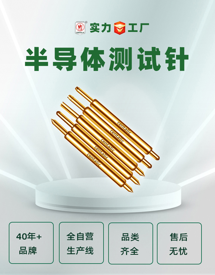
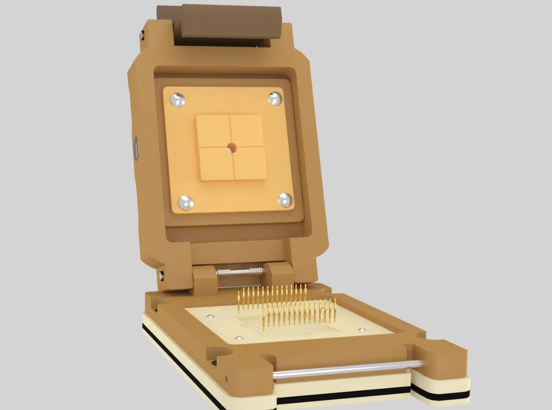
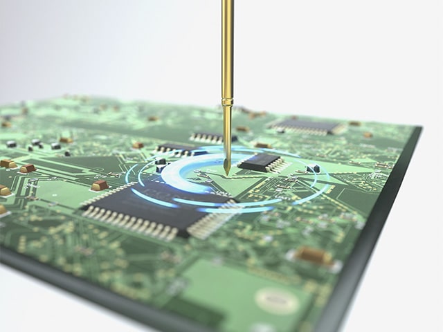
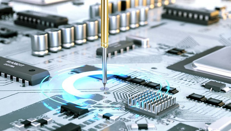
It connects one end to a chip pin (or wafer solder ball) and the other end to a testing machine, accurately transmitting electrical signals to detect the conductivity, current stability, functional integrity, and even aging performance of the chip in high temperature environments.
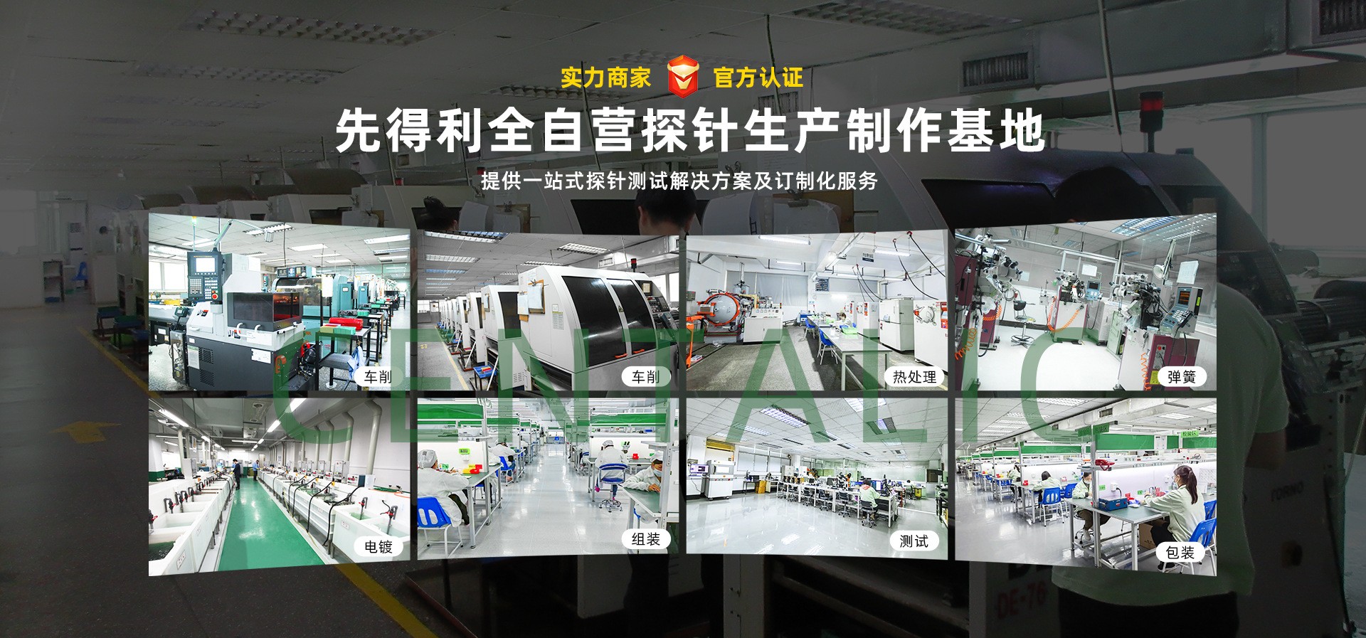
High density testing scenarios for AI chips often require probes of extremely small sizes. Centalic has been deeply involved in the field of testing probes for more than 40 years, with an integrated self operated production line that independently controls the entire process from raw material turning, cleaning, heat treatment, electroplating, assembly to inspection and shipment. This type of double headed probe can process a minimum needle diameter of 0.06mm and a needle tube diameter of 0.10mm, and also supports customization based on drawings and samples to meet testing needs with small spacing.
① If there are too many interfaces, there will be more needles
After the production of AI chips is completed, they cannot be directly assembled onto servers and must first undergo testing and verification. In the FT finished product testing process, the probe contacts the chip pins to achieve the transmission and reception of test signals. This may sound simple, but the pins of AI chips are becoming increasingly difficult to "dock", with a significant increase in the number of pins and a continuous reduction in pin spacing, resulting in longer testing times and higher requirements for probe contact accuracy.
The testing solutions for high computing power AI chips from different generations in the industry can intuitively reflect this change. The early testing solutions did not require the deployment of a large number of probes, while the testing solutions for the new generation of high computing power chips would require a doubled number of probes. The stronger the computing power of the chip, the more probes are required for supporting testing.
The high computing power AI chip has a huge instantaneous peak current. If only a small number of probes are used to carry high currents, voltage attenuation will occur, chip power supply will be unstable, and the final measured results will be inaccurate.
The engineering solution is to use a large number of probes in parallel to share the current. Equivalent to multiple water pipes carrying water together, the burden on a single needle is reduced, and voltage loss can be controlled, ensuring stable power supply during testing.
Chip testing is charged based on the testing time, and the longer the testing time, the higher the cost per chip. To dilute the testing costs of expensive AI chips, multiple test stations need to be set up on a probe card to simultaneously test multiple bare chips at once. Mobile phone chips have fewer pins per chip, and can be tested with dozens or hundreds of probes at once. However, a single AI chip itself requires a large number of probes, and some solutions support synchronous testing at multiple workstations, resulting in a significant increase in the total number of probes on the entire probe card.
Many people think that as long as there is enough space, simply stacking probes is enough. Reality is far from simple: tens of thousands of probes need to be pressed synchronously, and the contact pressure, stroke, and flatness of each probe must be strictly controlled. Insufficient pressure, contact resistance drift; Excessive pressure causes damage to the solder pads and rapid wear of the probes. The high current is concentrated in a narrow area, and the probe continues to heat up. Temperature changes will further interfere with the contact resistance, causing test drift. At the same time, the more needles there are, the higher the risk of single point contact failure, and the cost of probe card maintenance and repair also increases significantly. High end AI probe card is a comprehensive system that integrates mechanical, material, high-frequency electromagnetic, and thermal management.
The computing power of the first generation of AI chips will become increasingly powerful, with higher instantaneous operating currents and more high-speed signal interfaces. In the short term, the number of probes required for probe cards is likely to continue to increase.
The high-precision probe with small size and suitable ultra-fine spacing will continue to support the mass production verification of high computing power chips.