
Time:2026-09-09Reading:691Second
In the semiconductor industry chain, there is a type of component that is unremarkable: the diameter is often only a few tenths of a millimeter, and the needle tip is at the micrometer level, but it runs through the entire testing process of the chip from wafer to finished product. It is called a test probe. Many people wonder why we still rely on such small consumables when chip testing equipment is expensive and complex? Because the probe is the physical and electrical bridge between the testing machine and the chip, without it, the performance testing of the chip cannot be discussed.
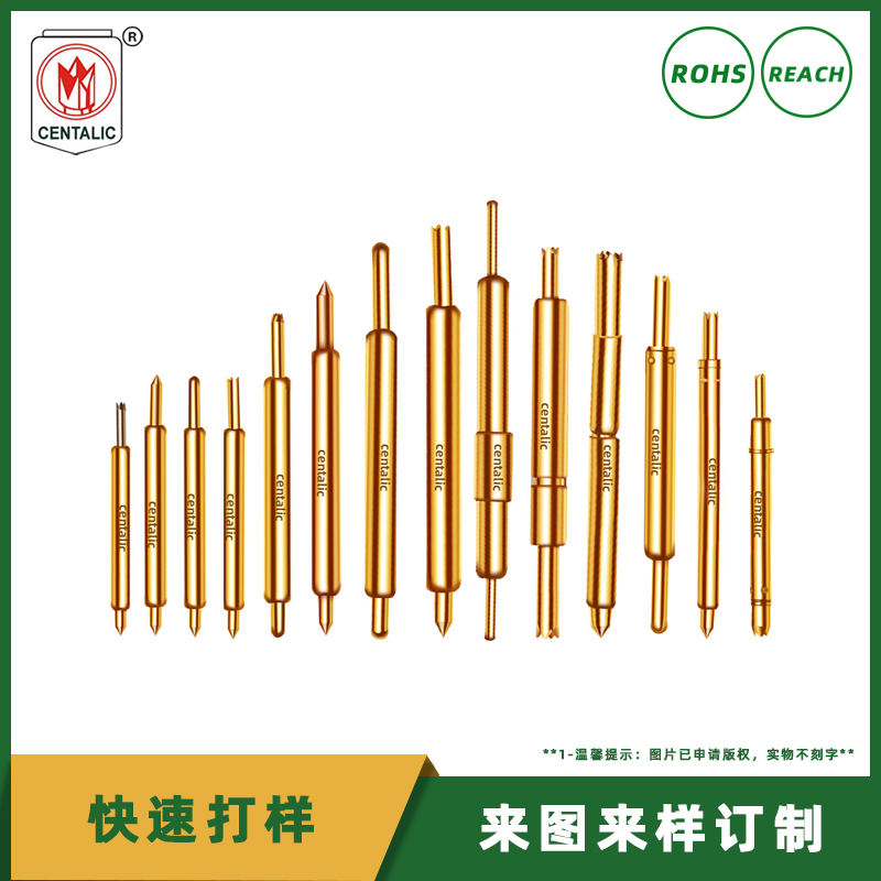
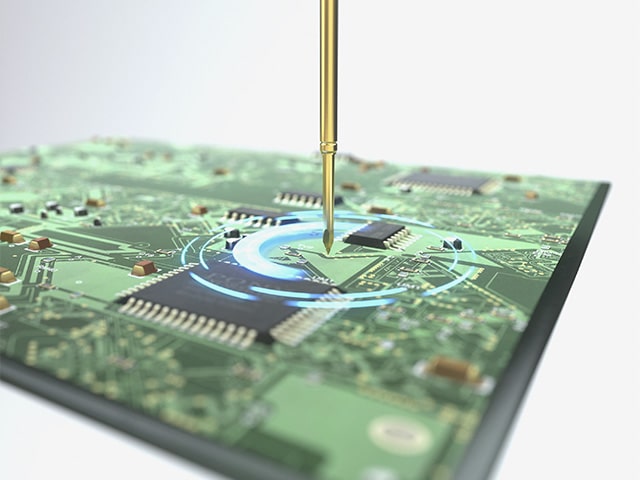
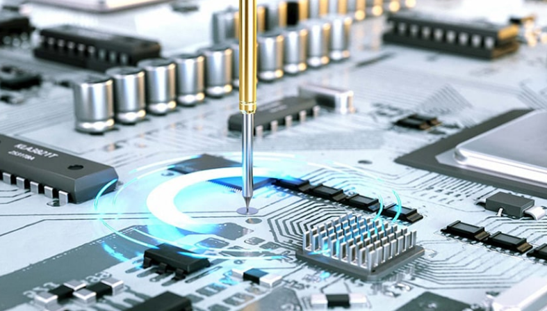
A probe generally consists of three parts: a needle, a needle tube, and a spring. In wafer testing or packaging testing, probes are installed on probe cards or test stands.When the probe is pressed down, the needle contacts the chip pad and contracts inward under force, compressing the internal spring. The deformation of the spring produces stable and controllable elastic force, ensuring that the needle firmly adheres to the pad and establishes a low impedance conductive path; On the other hand, it buffers the downward pressure impact force to avoid damaging the fragile solder pads of the chip due to excessive pressure. After the test is completed, the probe is lifted and the spring rebounds to reset, completing a complete test cycle. Electric signals are transmitted through needlesBi directional transmission of needle tubes, the voltage, current, high-frequency signals, etc. of the chip are transmitted to the testing equipment through probes to complete various performance tests of the chip.
2、 Building electrical bridges to achieve precise chip detection
The internal circuit of a chip is extremely precise, but the size of the solder pads and contacts is extremely small, and the circuit of the testing machine cannot be directly connected to the chip solder pads. The core mission of testing probes is to establish temporary and reliable electrical pathways.
Whether it is CP wafer testing at the wafer stage or FT finished product testing after packaging, it relies on probes to transmit voltage, current, high-frequency signals, etc., to read key parameters such as chip function, power consumption, conductivity, aging, etc., and determine whether the chip is qualified.
Without probes, no matter how powerful the testing equipment is, it is impossible to reach the micro contacts of the chip, and the quality of the chip cannot be determined.
3、 Double testing defense line, reducing costs, improving efficiency, and ensuring yield
The probe participates in two key "physical examinations" of the chip, directly determining the cost and yield of the production line.
Wafer CP testing:Pre packaging screening
The entire wafer has not been cut or packaged yet, and the probe card is equipped with hundreds or thousands of probes that can contact numerous bare chips on the wafer at once, screening out defective chips with manufacturing defects and functional failures in advance.
There is a consensus in the semiconductor industry that the earlier defects are discovered, the smaller the cost loss. If defective chips flow into the packaging process, all packaging materials and process costs will be wasted. Probes intercept defective products during the wafer stage, helping factories save packaging costs.
Finished FT testing:Final verification before leaving the factory
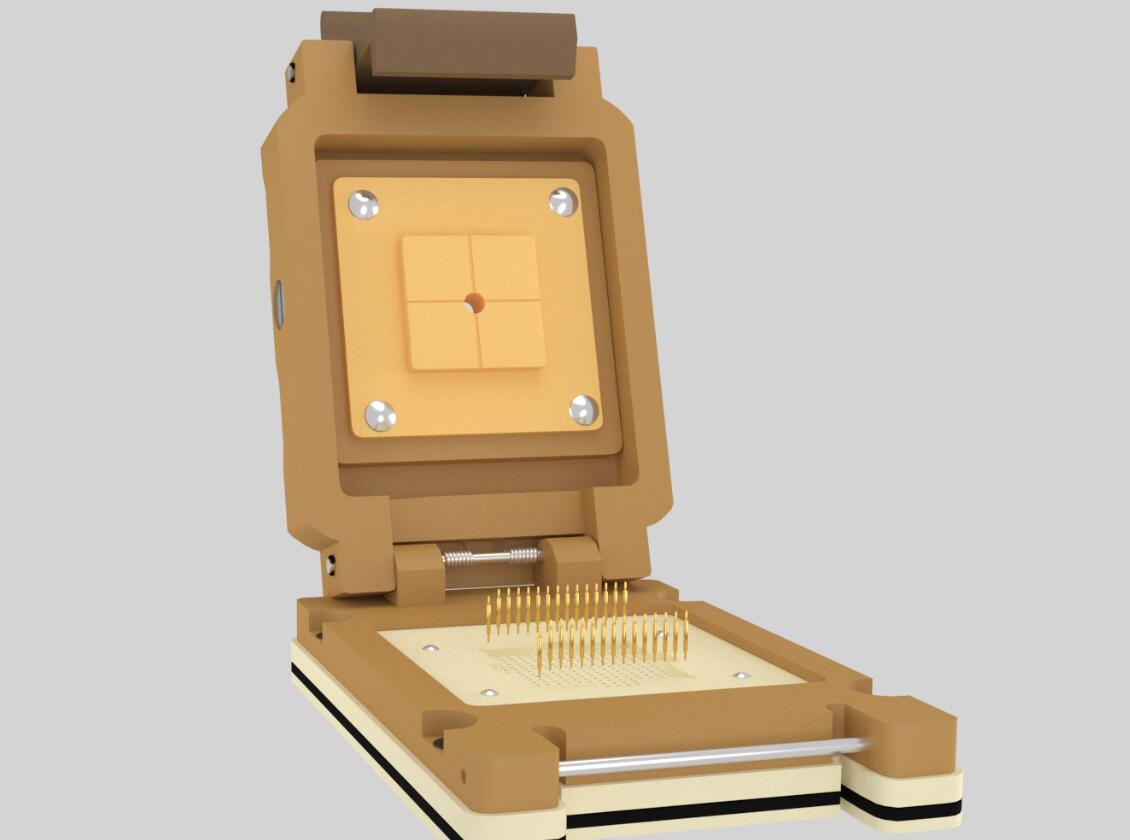
After the chip is packaged, the probe contacts the chip pins and solder balls in the testing fixture to complete a complete performance retest. Screen out new defects caused by packaging processes, ensure that every chip flowing into the market meets specifications, and avoid terminal equipment crashes, abnormalities, and other malfunctions.
In actual production on the production line, the probe status directly affects the testing yield. Needle tip wear, dirt, and unstable contact can cause contact resistance drift, resulting in a large number of misjudgments. Even qualified chips are judged as scrap, causing direct economic losses to the factory.

Although the probe is made of wear-resistant and anti-oxidation precision materials, every test is inevitably caused by the compression friction between the needle tip and the solder pad, resulting in wear and tear.
Mechanical wear and tear:Long term high-frequency reciprocating pressure testing,The needle tip will gradually grind flat and break corners, the coating will wear and fall off, the contact resistance will continue to increase, and the signal transmission will no longer be stable;
Accumulation of pollutants:Solder slag, flux, metal debris, and other attachments to the needle tip can cause false connections and false alarms during testing. Regular cleaning is required and replacement is necessary when the lifespan is reached;
Spring fatigue:After long-term high-frequency compression and rebound, the elasticity of the internal spring decays and the pressure becomes unbalanced, either damaging the chip pad or causing poor contact, resulting in test failure.
No matter how sophisticated the craftsmanship is, probes have a fixed service life and are consumables that must be replaced regularly. This is also the core feature that distinguishes them from ordinary equipment components.
With the continuous iteration of chip manufacturing processes, the size of solder pads is getting smaller and the pin density is exploding. AI chips, power devices, and high-frequency communication chips have put forward more stringent requirements for probes: they need to achieve micrometer level positioning accuracy while also considering the integrity of high-frequency signals, while not damaging the fragile solder pads of the chip.
Advanced process chip testing, probe tip size compressed to severaltenWithin micrometers, the manufacturing difficulty increases sharply. The iteration of probe technology synchronously supports the verification and mass production of the new generation of chips.
The test probe has a small volume and does not account for a high proportion of semiconductor material costs, but it is the throat component of the entire testing process. It does not produce signals, does not analyze data, but undertakes the most critical "contact" actions. Between each move, complete the quality screening of billions of chips. The small probe is the unknown gatekeeper of chip quality and the core consumable that cannot be replaced by semiconductor testing.
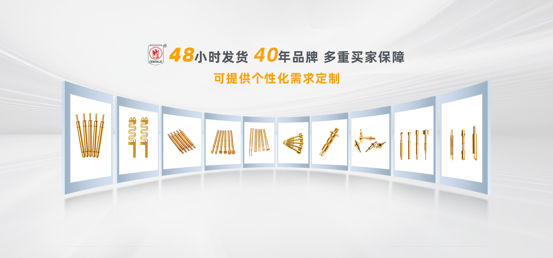
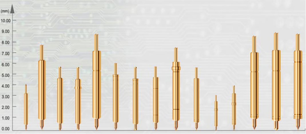
As one of the earliest national high-tech enterprises in China to produce large-scale testing probes, Suntory has been dedicated to probe research and development manufacturing for over 40 years, with independent control over the entire production process.The product is widely used for testing various electronic and peripheral products, covering areas such as semiconductor chips, mobile phone screen modules, camera modules, automation equipment, smart wearable home devices, medical equipment, automotive electronics, aerospace and military industries. In addition to standard products, it also supports customized testing probe services to serve customers from multiple industries, using domestically produced precision consumables to empower the high-quality development of the chip industry.