
Time:2026-08-19Reading:1531Second
In PCBA production testingIn the trial,By contacting the probes on the testing fixture with the PCB testing points, defects such as open circuits, short circuits, and incorrect component parameters can be quickly detectedHowever, the most common and headache inducing anomaly in actual production is none other thanPoor contact of ICT probe.Poor contact can lead to testing misjudgment, good products being judged as defective, repeated testing, decreased testing efficiency, and even affect the entire production cycle.
This article will start from the causes and systematically sort out a complete solution from rapid investigation, precise resolution to long-term prevention, to help enterprises improve testing stability and production efficiency.
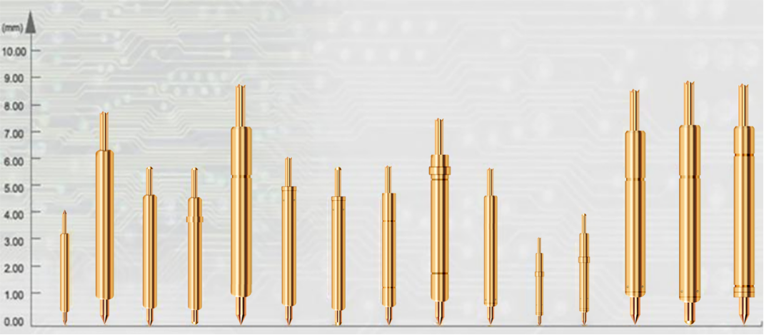
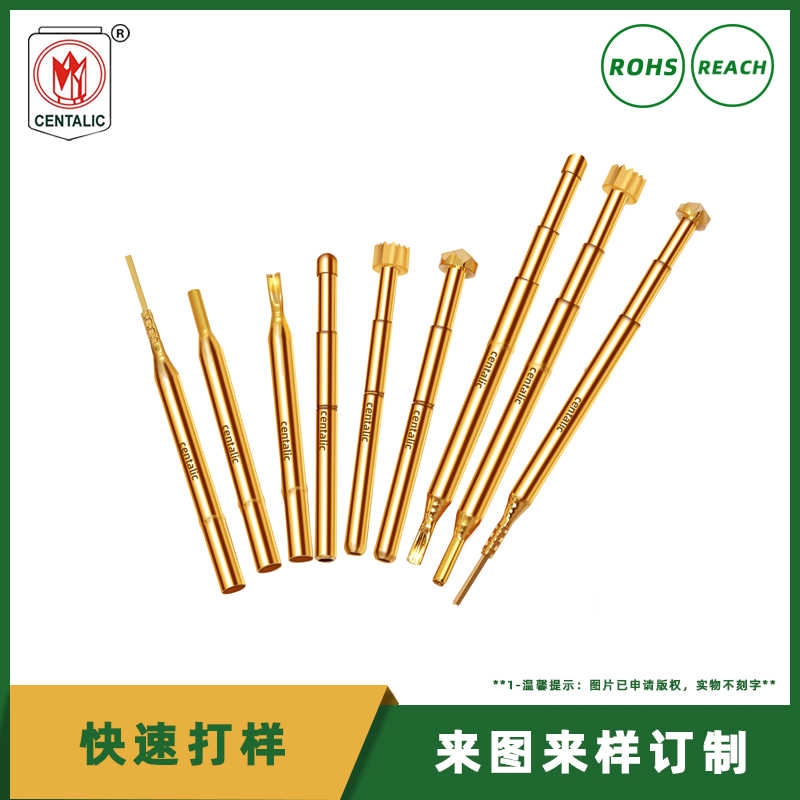
ICT probes, commonly known as ICT online testing probes, are precision electronic components. Its core structure consists of three parts:
syringe needle:Directly contact the critical parts of the tested device. The selection of its head shape will directly affect the effectiveness of the test.
Spring:Provide necessary contact force to ensure stable contact between the test needle and the test point.
Needle tube:As a supporting structure, it protects the internal springs and transmits signals.
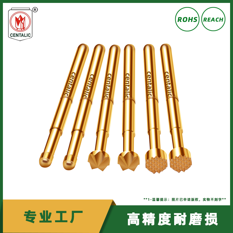
ICT probes are mainly used for online circuit testing and functional testing, detecting the electrical performance of online components on the board and the connection status of the circuit network. They can quantitatively measure and perform functional testing on the components.
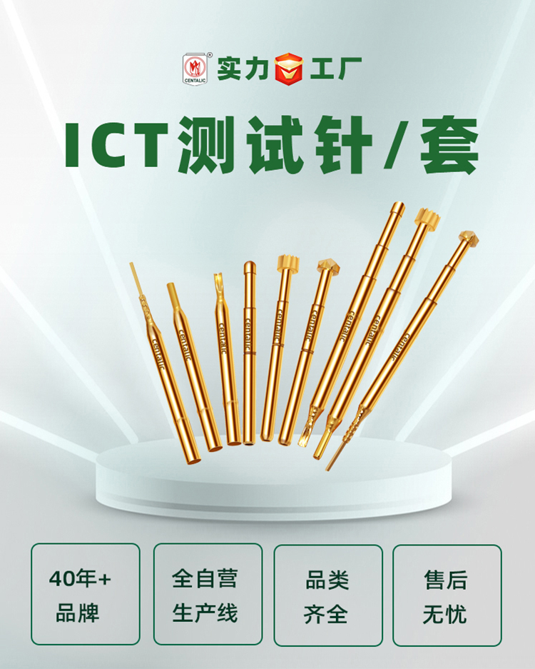
Generally,ICT probeUsed together with a matching size needle sleeve, the needle sleeve is fixed on the PCB board for easy replacement of probes at any time.
Poor contact of ICT probes is not caused by a single factor, but rather by the combination of multiple factors such as probe status, fixture performance, test object quality, and environmental conditions. Accurately identifying the cause is a prerequisite for solving problems.
As the core executing component of contact testing, the probe's state directly determines the contact effect. Long term high-frequency testing can cause wear and dullness of the probe tip. When the tip diameter wears from 0.1mm to 0.2mm, the contact resistance increases by 2-3 times; At the same time, the needle tip is prone to attachment of pollutants such as solder and dust, or oxidation in humid environments, forming an insulation layer that hinders current conduction; In addition, the fatigue of the internal spring of the probe can lead to insufficient elasticity, or the loosening of the needle seat can also cause unstable contact.
The stability of ICT testing fixtures is the foundation of reliable contact. The deformation of the bed bottom plate and the deviation of the support column can cause uneven force on the probe; Insufficient cylinder pressure or vacuum fixture leakage can cause the probe contact pressure to not meet the standard requirements; Improper setting of probe contact pressure (too large can easily damage the needle tip and solder pad, while too small cannot form effective contact) is also a common equipment factor that causes poor contact.
The test point is the contact carrier of the probe, and its design and quality directly affect the contact effect. If the diameter of the test points is too small, the spacing is too dense, or the solder pads are covered by solder mask during the design phase, it will increase the difficulty of precise probe contact; The storage environment of PCB boards is humid and prolonged, which can lead to surface oxidation of test points and the formation of high resistance oxide layers; However, if the PCB board is bent or pressed unevenly, or if there are dents or deformations in the test points, some test points may not be able to effectively adhere to the probes. In addition, residual solder flux, oil stains, fingerprints and other pollutants on the surface of the PCB board can also hinder the ohmic contact between the probe and the test point.
The interference of static electricity, temperature and humidity fluctuations in the testing environment can indirectly affect the stability of probe contact. Static electricity can cause test signal drift. Environmental humidity exceeding 60% can accelerate the oxidation of the test point and probe, while humidity below 30% can easily generate static electricity; At the same time, poor grounding of the test bench can introduce noise interference, resulting in test data jitter.
Strictly follow the production line treatment for the four major causesFirst investigate and then rectify, first low cost and then high investment, first mechanical and then softwarePrinciple: Eliminate blindly modifying test thresholds to cover up hardware issues and solve poor contact from the root.
1. Probe status investigation:Observe the probe tip with a microscope at a magnification of over 50 times to check for wear, dullness, oxidation, deformation, and other issues; Gently pull the tail of the probe and check if the needle cover is loose or detached; Wipe the needle tip with a clean cloth dipped in anhydrous ethanol. If the contact stability is significantly improved after wiping, it can be determined as a needle tip contamination problem.
2. Stress investigation:Use a pressure tester to measure the probe contact force and ensure that the probe contact force matches the corresponding model standard parameters.
3. Test points and PCB troubleshooting:Visually zoom in and observe the measuring points: check for oxidation, contamination, and deformation, and also inspect whether the PCB board is bent or unevenly pressed.
4. Environmental and grounding investigation:Confirm that the test bench is level and free from shaking, and that the equipment is firmly and reliably grounded;Confirm that the temperature and humidity in the workshop are maintained within the standard range, with no significant vibration or electromagnetic interference from high-power equipment.
1. Probe and needle cover protection:For probes with severe wear and oxidation, replace them directly; Probes with slight contamination can be wiped and cleaned with anhydrous ethanol; For probes with insufficient elasticityReplace the entire needle; Mass production fixtures require regular preventive replacement of probes based on production conditions.
2. Fixture and equipment calibration:Correct or replace the deformed bed bottom plate, and tighten the support columns and interface connectors; Calibrate cylinder pressure and vacuum fixture sealing to ensure stable probe contact pressure;
3. Testing points and PCB quality improvement:For oxidation and pollution testing points, the oxide layer and pollutants need to be removed; PCB finished products are packaged with moisture-proof materials, and the humidity of the workshop storage environment is strictly controlled; Flatten bent PCB boards and scrap those with severe deformation.
To solve the problem of poor contact of ICT probes, it is not only necessary to "treat the symptoms", but also to "treat the root cause". By establishing a full process prevention and control system, the incidence of poor contact can be significantly reduced.
PCB pre design synchronous docking testing project: standardize the size and spacing standards of test points to ensure that the test points are transparent without solder mask coverage; Reasonably layout the testing point positions to facilitate precise contact of probes. Good DFT design can reduce the risk of poor contact from the source.
3. Maintenance end: Establish a regular maintenance mechanism
Develop a detailed equipment and fixture maintenance plan: daily inspection of probe status and cleanliness; Conduct a comprehensive inspection and calibration of the probe card and needle bed bottom plate once a month; Regularly check the operation status of the grounding system, ion fan, and temperature and humidity equipment to ensure effective environmental control. At the same time, establish records of probe replacement and maintenance to achieve full lifecycle management.
Poor contact of ICT probes is a common but easily overlooked "invisible killer" in the testing process. From the wear and contamination of the probe itself, to fixture positioning, PCB design, and even environmental interference, every detail can become a trigger for misjudgment. By implementing a closed-loop management system that integrates design optimization, process control, standardized operations, and regular maintenance, enterprises can significantly reduce the incidence of poor contact, improve testing throughput, and enhance product quality stability. As a national high-tech enterprise with a fully self operated large-scale probe production line, Centalic has been deeply involved in the research and manufacturing of testing probes for more than 40 years,Having a deep understanding of the pain points in mass production testing, we provide support for closed-loop control of the production line with our self-developed and self-produced high-quality probe hardware.
A small probe is worth your systematic attention - it returns lower misjudgment rates, higher production line efficiency, and more reliable product reputation.