Time:2025-09-05Reading:638Second
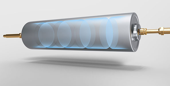
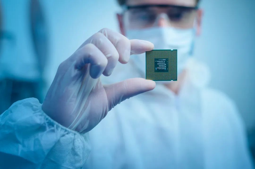
Semiconductor testing needles are generally formed by precision instrument riveting and preloading of three basic components: needle tip, needle tube, and spring. Due to the small size of semiconductor products, especially chip products, the size of probes is required to reach the micrometer level, which is a high-end precision electronic component with high manufacturing technology content. During wafer or chip testing, probes are generally used for precise connection between wafer/chip pins or solder balls and the testing machine, to achieve signal transmission and detect performance indicators such as conductivity, current, functionality, and aging of the product.

What are the applications of semiconductor testing needles in the semiconductor industry chain?
Semiconductor testing needles are mainly used in wafer testing and chip testing in the semiconductor industry chain.
The semiconductor industry chain includes stages such as chip design, manufacturing, packaging, and testing. Semiconductor testing needles mainly serve the wafer testing and chip testing stages.
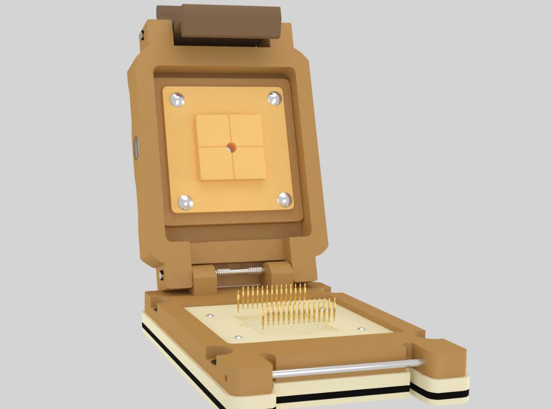
In the wafer testing process, the probe card comes into contact with the bare chip pads on the wafer, and the electrical performance of the chip is detected through electrical signals to screen for non-conforming products and reduce packaging costs;
In the chip testing stage, probes are used for finished product testing after packaging, including performance testing, reliability testing, etc. They need to be adapted to pins or solder balls of different packaging forms, and verify the performance stability of the chip in actual working scenarios through high-frequency and high-precision signal transmission. In these two stages, the conductivity and wear resistance of semiconductor probes will directly affect the efficiency and accuracy of semiconductor product quality screening.
Driven by Moore's Law, the chip manufacturing process has undergone a leapfrog development from micrometer to nanometer. What impact will the miniaturization of chip manufacturing processes have on the semiconductor testing needle industry?
The evolution of chip manufacturing processes drives the semiconductor testing needle industry towards high precision and high performance!
In the 1960s, Moore's Law predicted that the number of transistors that could be accommodated on integrated circuits would double every 18-24 months, and performance would also double accordingly. This prompted the semiconductor industry to continuously break through physical limits and pursue smaller and more efficient chip manufacturing processes. Driven by Moore's Law, the chip manufacturing process has achieved a revolutionary leap from micrometer to nanometer. In the 1970s and 1980s, processes above 1 micron were the main focus. With the iteration of photolithography and etching technology, chip processes gradually shrank to 0.35 microns and 0.18 microns by the 1990s. After entering the 21st century, chip processes entered the nanoscale. Taking TSMC, a leading global chip manufacturer, as an example, in 2004 TSMC achieved mass production of the 90 nanometer process. Subsequently, it continued to accelerate technological innovation and successively achieved mass production of key nodes such as 65 nanometer, 45 nanometer, 40 nanometer, 28 nanometer, and 20 nanometer; In the mid-2010s, TSMC's chip manufacturing process further broke through to 16nm, 10nm, 7nm, and 5nm. It successfully mass-produced the 3nm process in 2022 and is expected to advance the production of the 2nm process by 2025. In summary, TSMC's efficient and stable process iteration progress will help promote technological innovation and development in the semiconductor industry, and drive continuous improvement in chip performance.
With the evolution and development of chip manufacturing processes, the design of semiconductor devices is becoming increasingly complex and refined, which in turn drives the semiconductor testing needle industry towards high precision and high performance. On the one hand, as the chip manufacturing process shrinks from the micrometer level to the nanometer level, the number of transistors on the chip increases exponentially, while the size of individual transistors decreases significantly. This means that the circuit nodes and pin spacing on the chip also become smaller and denser, requiring smaller test probes to achieve effective contact and testing of these micro components; On the other hand, advanced process chips have strict requirements for the accuracy and stability of signal transmission, requiring probes to have good conductivity and mechanical strength to meet high-frequency and high-speed signal testing. Therefore, the advanced development of chip manufacturing processes will become an important driving force for the development of the semiconductor testing needle industry. In order to meet the cutting-edge demands of chip manufacturing, semiconductor testing needles will continue to innovate and optimize in structural design and material selection, driving the overall evolution of the industry towards high-end direction.
What impact will the increase in integrated circuit production have on the probe industry?
The growth of integrated circuit production in China will drive the synchronous expansion of the semiconductor testing needle market.
In the past decade, China's integrated circuit industry has developed rapidly, with output showing a rapid growth trend. According to statistics from the National Bureau of Statistics, China's integrated circuit production increased from 101.55 billion pieces to 451.42 billion pieces from 2014 to 2024, with an average annual compound growth rate of 16.1%. Due to the multiple testing stages that each integrated circuit undergoes from wafer manufacturing to chip packaging, semiconductor test pins are key consumables in the integrated circuit manufacturing process. Therefore, as the output of integrated circuits increases, the demand for test probes also increases synchronously.
Driven by the booming development of emerging technologies such as 5G communication, artificial intelligence, and the Internet of Things in the future, the demand for high-performance and low-power chips in various fields will increase significantly, which will further stimulate the growth of integrated circuit production and provide strong impetus for the expansion of the semiconductor testing needle market.
First profitFocused on probe research and production for over 40 years, we are a company with a fully self operated scaleWe are a national high-tech enterprise specializing in the research, development, and manufacturing of various types of testing probes. Centalic can process the minimum semiconductor testing needle diameter: needle diameter: 0.06mm/needle tube diameter: 0.10mm.