Time:2026-02-09Reading:1316Second
According to media reports, Samsung Electronics has made key progress in localizing its semiconductor layout in the United States.
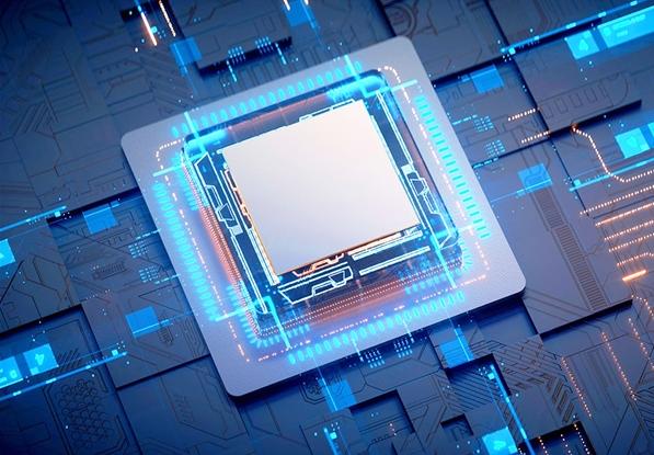
Samsung Electronics has received temporary approval to initiate partial operations of its chip factory under construction in Taylor, Texas. This marks a substantial step forward in its plan to produce the next generation of AI chips for Tesla.

According to the temporary occupation permit obtained, Samsung can use approximately 88000 square feet of the Taylor factory area in advance. The factory is expected to start large-scale production in the second half of this year, with the primary task of manufacturing AI5 chips for Tesla and plans to produce AI6 chips in the future.
Tesla CEO Elon Musk previously stated that the AI5 chip design is nearing completion and has developed an aggressive roadmap to shorten the AI chip design cycle to 9 months.
The factory construction is progressing according to plan, and it is reported that Samsung plans to start testing extreme ultraviolet lithography equipment next month, which is the key to producing advanced 2-nanometer processes. The entire factory area is expected to complete 6 million square feet of construction by the end of this year, and plans to add another 1 million square feet by 2028, with a total park area of over 1200 acres.
In addition to serving Tesla, Samsung's wafer foundry business is actively expanding to more American customers to meet the rapidly growing demand for artificial intelligence and high-performance computing chips. The company's goal is to achieve a growth of over 130% in orders for 2-nanometer chips this year.
At the same time, its competitor TSMC is also accelerating its layout in the United States. It is reported that it is considering expanding its Arizona factory to a total of 11 and will also participate in the production of Tesla AI5 chips.