Time:2025-06-02Reading:1003Second
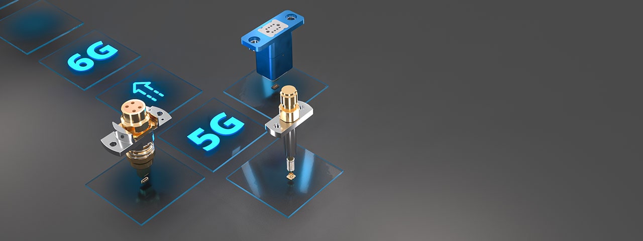
In the field of semiconductor subdivision, every tiny component carries an important mission, and semiconductor test probes are among the most important components. It plays a key role in ensuring chip quality, playing a core role in signal transmission during chip design verification, wafer testing, and finished product testing, and playing an important role in quality control of semiconductor products.
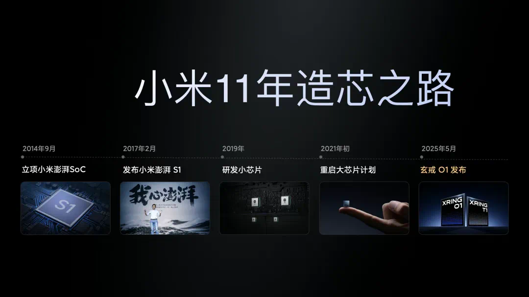
On May 22, 2025, Xiaomi launched the Xuanjie brand at its 15th anniversary strategic launch eventO1Chips have intricate connections with semiconductor high-frequency needle technology, jointly outlining the innovation blueprint of the semiconductor industry.
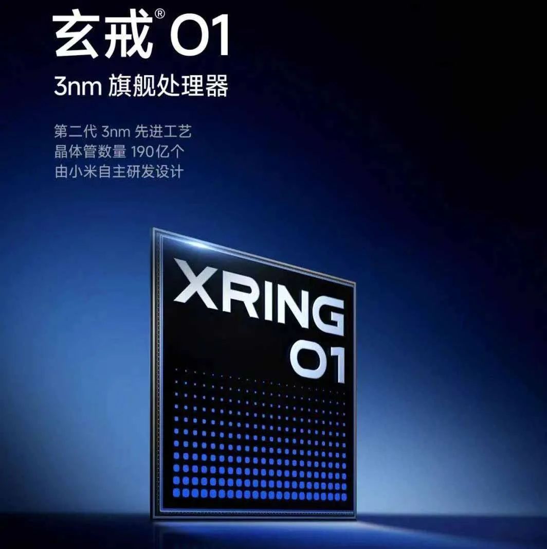
Xuanjie O1 chip: the peak of domestic chips
The birth of the Xuanjie O1 chip marks a milestone step for Xiaomi in the field of chip research and development, and is also an important node in the development of China's semiconductor industry.Using TSMC's second-generation 3nm process chip, 19 billion transistors are integrated in a space of 109mm ², achieving a breakthrough balance between performance and energy efficiency with a 10 core four cluster architecture.
What is a semiconductor test probe?
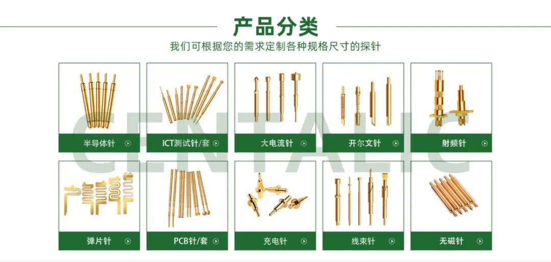
According to different application fields, the probe market can be subdivided into semiconductor testing probes, ICT testing probes, high current probes, Kelvin probes, RF probes, shrapnel probes, PCB spring needles, charging needles, non-magnetic probes, and other types. Among them, semiconductor testing probe technology has higher difficulty, not only in terms of finer size, but also in terms of more functional testing requirements.
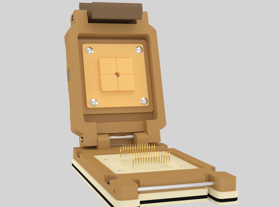
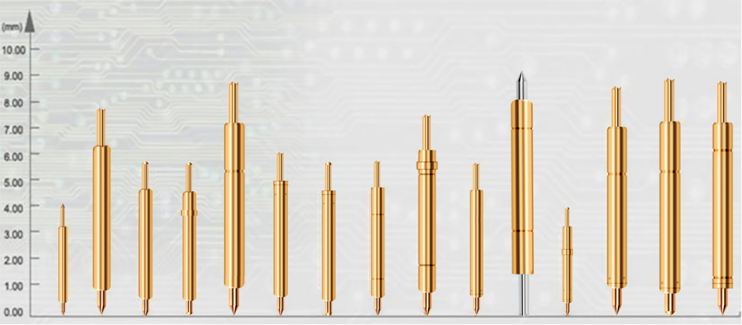
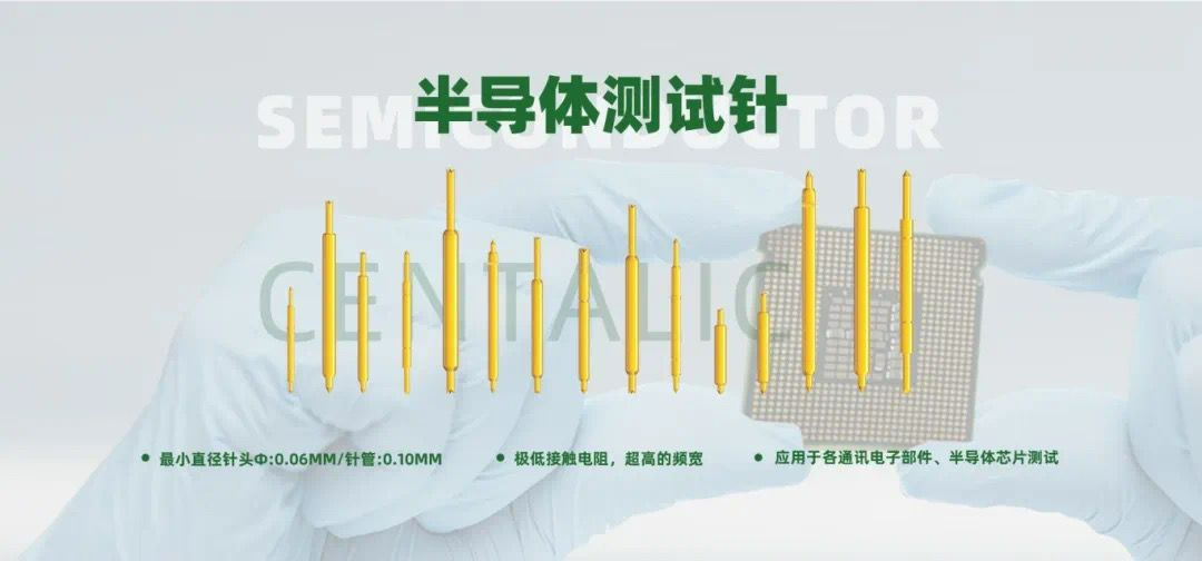
Semiconductor testing probeAlso known as dual head probeUsed for electrical performance testing during the chip manufacturing process. They are usually able to accurately transmit electrical signals with a very small contact area. The main functions of the probe include:
Contact chip pads or pins to establish temporary circuit connections;
Transmitting test signals to detect the logic function, current, voltage and other parameters of the chip;
Screen defective products to ensure that only qualified chips enter the next stage.
Due to the increasing integration of chips, the size and accuracy of probes must also be improved accordingly. For example, in chip testing using 5nm or even 3nm processes, the tip diameter of the probe may only be a few micrometers, several times finer than a human hair.
How can probes become the 'golden fingers' of chip manufacturing?
In the chip testing stage, there are usually hundreds or even thousands of probes arranged on the probe card, which gently touch the chip pads like "golden fingers" to complete signal acquisition. This process is similar to a magician touching the runes of a magic circle with their fingers to activate their power.
Wafer testing:Before chip cutting and packaging, the probe card will test each chip on the entire wafer, mark defective products, and avoid wasting packaging resources in the future.
Final testing:After the chip packaging is completed, the probe undergoes strict testing again to ensure its stability in real environments.
If the contact of the probe is poor or the accuracy is insufficient, it may lead to misjudgment, causing good products to be discarded or defective products to flow into the market, resulting in huge losses. Therefore, the manufacturing process of the probe directly affects the final quality and cost of the chip.

Industrial Collaboration: Refactoring the Domestic Testing Chain Behind Xuanjie O1
The success of Xuanjie O1 indicates the initial formation of a complete technical closed loop for domestic chips from design to testing
Evolution of market pattern
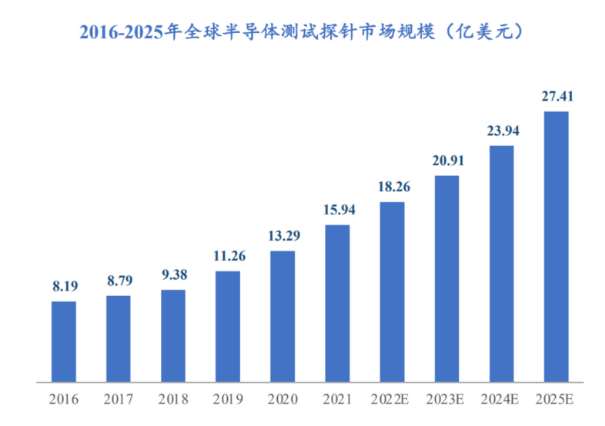
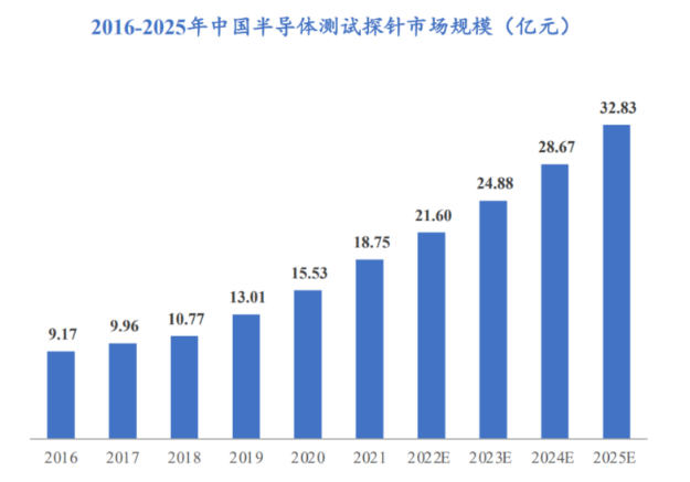
The global testing probe market has grown from 1.594 billion US dollars in 2021 to 2.74 billion US dollars in 2025, and the market share in China has increased from 1.301 billion yuan in 2019 to 3.283 billion yuan in 2025;
The domestic packaging and testing industry accounts for over 40% of the global market, driving a surge in demand for local probes. Companies such as Huacheng Chuangke and Kangster have achieved mass production of 10 μ m probes, gradually replacing international manufacturers such as Advantest in Japan and FormFactor in the United States.
Localization empowerment path
Policy driven: The proportion of investment in testing equipment and key components by the National Development Fund Phase II has increased to 15%, promoting the autonomy of probe materials and processing equipment;
Technical collaboration: Xiaomi and other chip design companies jointly establish a joint laboratory with Changdian Technology, Huatian Technology and other packaging and testing factories to optimize the chip DFT (Design for Testability) by reverse engineering probe test data, such as improving the electrostatic protection circuit design of Xuanjie O1 through ESD failure mode feedback from probes.
From the stunning debut of Xuanjie O1 to the thriving development of the global semiconductor industry, semiconductor testing probes have always played a key role behind the scenes. With the continuous improvement of China's semiconductor industry chain, domestic probe companies are ushering in a historic opportunity. This' golden key 'to the world of chips will continue to unlock a new era of more precise and intelligent semiconductors.